Such a great build Vunce!
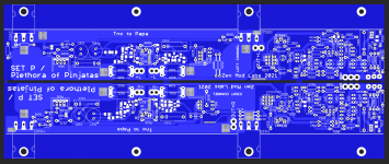
So compact M2 board.
I have been running both my SMPS-powered F6 and M2X without a fan, so far no issues.
Because at late-night listening, I can still hear the fan buzz, so I remove the fan completely.
You may want to try running without Cap-Bank first then add capacitance to your liking.
Looking forward to hearing your reviews on your M2.
More M2 progress 🙂
Both M2 amp boards were powered up from my bench power supply and seem healthy. There is a lengthy delay and slow ramp up before the amp modules reach their working bias current.
Both amps were built exactly the same, but amp #1 draws 1.5A and amp #2 draws 1.32A??
Very close for music to flow.....
@ Vunce
Great setup you have.
It's better to use a fan where possible, a super silent fan like the one I used for you won't generate any noise at all. Also, it will help to cool down the transformer for + 3A current.
SMPS500-CLA will run normally without a fan, so no worries at all.
Thanks!
After a long pause on this M2 project, it's back on the workbench. I left off tracking down a bit of hum that's not acceptable and a difference in bias current between amp boards.
Chan #1 = 1.35A
Chan #2 = 1.7A
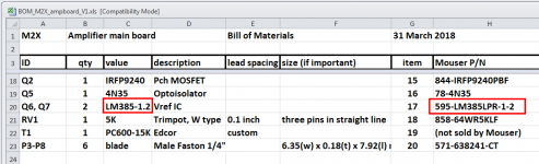
I started poking around and comparing the schematic for this M2 version versus others and noticed this amp has LM385-2V5 spec'ed in the BOM instead of LM385-1V2.
Increasing the LM385 clamping voltage will affect the optocoupler LED and the output bias setting and therefore should be replaced with 1V2's, correct?
Chan #1 = 1.35A
Chan #2 = 1.7A
I started poking around and comparing the schematic for this M2 version versus others and noticed this amp has LM385-2V5 spec'ed in the BOM instead of LM385-1V2.
Increasing the LM385 clamping voltage will affect the optocoupler LED and the output bias setting and therefore should be replaced with 1V2's, correct?
it must be 1V25, or no function
it is "just" safety for optodiode, it goes Kaput with higher voltage
if you have discrepancy in Iq between channels - replace opto - no other possible reason if all resistors are of proper value
source resistors - voltage sag across them is firing up optodiode
it lits, opening optotransistor, it allows current trough resistors from rails to gates ( C-E of optotransistor)
optotransistor more open, higher current trough said resistors, greater voltage sag across them , gates goes closer, closing mosfets, decreasing voltage sag across source resistors .....
simple .......... when someone got idea, chew it and spit on ya for free
Yup, this will explain the wacky behavior. Correct value parts will be on order asap.
Thanks ZM! 😉
Thanks ZM! 😉
I am using same power supply x 2 for Sissy sit Vunce can you show me your grounding scheme when you get a sec. I have no clue how to integrate safety ground with SMPS or just to leave them isolated.
Prasi nice integration smt and through hole, we need to start moving away from through hole as they just drying up supply.With proper soldering equipment I have been enjoying it.
Bill
Prasi nice integration smt and through hole, we need to start moving away from through hole as they just drying up supply.With proper soldering equipment I have been enjoying it.
Bill
Last edited:
Hi Bill,
Currently my M2 is disassembled because I have to replace a few incorrect components. Probably replace the optocouplers while I'm in there also just in case they were damaged.
As far as grounding the SMPS, the aluminum plate is tie to the AC side of the psu through a corner brass standoff. For the DC side, I have good results connecting an NTC (CL60 or similar) in series between a GND tab and chassis star ground point. I tested this SMPS with my Alpha20 amplifier with this same scheme and it was dead quiet.
This amp had a slight audible hum, but I unknowingly had other issues going on. When my M2 back together, I will investigate further if there is still hum present.
I have grown very fond of the SMT soldering also! It is the future for our great hobby. With a few key tools ( magnifying headgear, Tweezers, Fine tip iron) most basic builds can be tackled without issue.
@ZM
Thanks for the additional reading how the opto bias circuit works 😉
Last edited:
smd is good when space is of premium importance
if that's not the case , I'm not bothering ...... after all these years I'm still enjoying in bending leads of parts on that plastic thingie and cutting them later
of course, that's just me - if your Zen is more, when soldering tiny bugz, who am I to dispute 🙂
though, see this - space
if that's not the case , I'm not bothering ...... after all these years I'm still enjoying in bending leads of parts on that plastic thingie and cutting them later
of course, that's just me - if your Zen is more, when soldering tiny bugz, who am I to dispute 🙂
though, see this - space
Attachments
Babelfish M25/SET with active FE (instead of autoformer FE) and biasing circuit stolen from Babelfish XA252
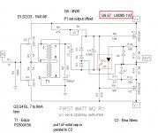
Before I removed the M2 boards from the heatsinks I wanted to get voltage measurements from key test points with the LM385-2v5 (D4, D5) reference diodes in place. I marked up the schematic with the recorded measurements. All points but (A) look slightly off from a properly tuned M2. I double checked all resistors and components for correctness - all good but the LM385’s. Would the incorrect ref diodes cause the wonky voltages at points (B) and (C)?
(Note: P2 trimpot is not installed on my boards.)
(Note: P2 trimpot is not installed on my boards.)
Attachments
measurements from key test points with the LM385-2v5 (D4, D5) reference diodes
somehow that doesn't sound quite right; here are a couple of images
_
Attachments

Yes, the incorrect LM385's were installed. I have the correct LM385-1v2 on the way (same LM385's as in your M2x BOM), I wanted to get a "state of health" report on the patient before the components are changed.
Last edited:
Vunce,
Thanks same as regular power supply then.I always cringe when things don’t work properly but always come back with a better understanding once corrected. I guess that is what keeps us going.
Bill
Thanks same as regular power supply then.I always cringe when things don’t work properly but always come back with a better understanding once corrected. I guess that is what keeps us going.
Bill
Last edited:
....Would the incorrect ref diodes cause the wonky voltages at points (B) and (C)?
....
I did replied to that question specifically
Update
Tonight I removed the 4N35 and LM385-2v5’s and replaced them with a new 4N35 and the correct LM385-1v2’s in channel #2. This was the channel that had 0.712mV across R14.
After the component swap, the voltage across R14 was 0.603mV. All the other test point voltages from the attachment on post #133 are almost exactly the same. So this exercise lowered the bias current to approximately 1.3A, but didn’t change the voltages at the JFETS or Optocoupler pins 1-2, 4-5?
Attachments

Yup, bias current is bang on now 🙂
I was questioning the unequal Jfet source voltages and small dc voltage at the Edcor input. But, more reading through the various M2 threads has answered my concerns. It seems the matched pairs of JFETs I had in my stash are not so closely matched after all. Removing R3/R4 and installing a trimpot “hack” from post #2592 of the ‘Official M2 schematic’ thread will null the dc offset. The nice part is Prasi included a location on the pcb for this adjustment trimpot (P2) without having to remove R3/R4.
The journey never ends…. 😉
- Home
- Amplifiers
- Pass Labs
- Nelson Pass M2