AndrewT said:No.
R1 sets the total current for the LTP pair.
R1 does not set a balanced current through the pair.
post 97 is still not being understood.
Because it´s simply wrong.
"The adjustment is there to balance the FET currents"
No it´s there to balance the BJT currents.
If you would like to balance the FET currents (to correct for unmatched FETS), the only way to do this would be by source resistors.
The collector resistors have an impact on the current of their corresponding BJTs only.
I give up.
GK either go and build it and measure it, or simulate it and get the sim to measure the effects.
GK either go and build it and measure it, or simulate it and get the sim to measure the effects.
AndrewT said:I give up.
GK either go and build it and measure it, or simulate it and get the sim to measure the effects.
I´m certainly going to build it. BTW: HKC who started this thread has built a variant of it, and strange enough, as turned out in a conversation with private mail, his measured operating points correspond to what I say.
There are a several variants of this circuit found in equipment built by Parasound,
and obviously the all work without "balancing the FET currents by adjusting the collector resistor of the following stage".
Increasing the current through the output devices:
I have read that in the original circuit the output devices run at 25mA per devive.
I will have to run the Toshiba parts at a slightly lower current than the original
ones, but 10mA per device should be ok for the V Parts. I have increased the drain resistors
(R2, R3) to 133 Ohms, so there will be a voltage of 1.33 V across them.
If we assume a Vbe of approx. 0.6V for the BJTs (Q5, Q6) and look at the R8, R9, R4
assembly like it would be a single 20 Ohms restistor like R5 is, then the current
through this resistors would be approx. 36.5 mA. 10mA of this go to Q2 (and Q4 on the negative
half) leaving approx. 26.5 mA for Q5 (and Q6 on the negative half). They will dissipate
0.43W then.
Attachments
gk7 said:Increasing the current through the output devices:
I have read that in the original circuit the output devices run at 25mA per devive.
I will have to run the Toshiba parts at a slightly lower current than the original
ones, but 10mA per device should be ok for the V Parts. I have increased the drain resistors
(R2, R3) to 133 Ohms, so there will be a voltage of 1.33 V across them.
If we assume a Vbe of approx. 0.6V for the BJTs (Q5, Q6) and look at the R8, R9, R4
assembly like it would be a single 20 Ohms restistor like R5 is, then the current
through this resistors would be approx. 36.5 mA. 10mA of this go to Q2 (and Q4 on the negative
half) leaving approx. 26.5 mA for Q5 (and Q6 on the negative half). They will dissipate
0.43W then.
I have 1v across R4 & R5 20 Ohm resistors = 50ma @ output stage and I had tested before it sounds better than when it was @ 30ma.
You guys worry too much. The bias adjustment changes BOTH the input fets and the output Bipolars. Bipolars are most important to adjust.
john curl said:You guys worry too much. The bias adjustment changes BOTH the input fets and the output Bipolars. Bipolars are most important to adjust.
thank you.
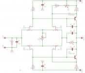
John is correct 🙂 Here's exactly how this circuit is working. Looking at the http://www.diyaudio.com/forums/attachment.php?s=&postid=1758854&stamp=1235749661 schematic:
- A JFET in saturation acts as a costant current source; the current is defined by Idss and Rsource. Here, Rsource is R1 therefore R1 defines the current through R2 and R3.
- Assuming all JFETs are matched, looking only at the upper half, neglecting base currents and also assuming the Q1...Q4 bias is 10mA: the voltage drop across R2 is 1.33V.
- Substract 0.65V and the voltage across R4 is 0.68V. Therefore the current through R4 is about 20mA. This is not the Q5 collector current.
- The Q5 collector current is the difference between the current through R4 and the Q2 drain current: 20mA-10mA=10mA.
- The same applies on the lower half. Hence, ideally, if Q5 and Q6 would be perfectly matched, IQ6=10mA and the output is at zero volts.
- However Q5 and Q6 are barely identical; overall, the DC gain of this circuit is pretty high and the slightest imbalance would flip the output DC towards the rails.
-Here comes R6 closing the negative feedback loop and providing a DC return path for the input stage. Assume the output goes toward the positive rail. The JFET gate current is always almost zero, therefore the voltage at the Q2 and Q4 gates copies the output voltage. Raising the gates voltage increases the current through Q2 and decreases the current through Q4. As long as the current through R4 and R5 is constant, this means the current through Q5 decreases and the current through Q6 increases. Therefore, the output voltage would decrease, hence the negative feedback effect. The output has no other chance then staying at exactly 0V (again, if Q1...Q4 are perfectly matched).
- Then what is R9 doing? It obviously adjusts the current through Q5 and Q6. However, adjusting R9 will also trigger a change in the Q1...Q4 currents (because the current flowing through R9 can be provided by Q2 only). So you can also look at R9 as a Q1...Q4 balancing pot. Obviously, balancing Q1...Q4 will minimize the distortions, hence the "IMD" labelling on R9. The balance will act as while Q2/Q3 current goes up, Q1/Q4 current goes down.
- Now, the bad news... The main problem with the schematic you provided is the poorly defined AC gain. The AC gain is defined by R6 and the input impedance of the right JFET pair. This is poorly defined... Don't know who designed this schematic but this is not exactly the JC-2 preamp! JC-2 uses this schematic as a discrete opamp, with the right pair gates as the inverting input. You need to define a feedback network around the inverting input and use the whole amp in a non-inverting configuration. Because of R6 (providing a DC return path), the feedback loop can be AC only.
"You need to define a feedback network around the inverting input",
yes of course. But this feedback network already exists in the ML-1 (located on the mainboard), the schematic only shows whats inside the plugable line modules. BTW your explanation of the circuit does not differ from mine me thinks. Except that you assumed a higher Vbe of 0.65, resulting in lower voltage accross R4 and thus only 20mA per output device, which would be to low compared to the original, maybe the drain resistors could be increased a bit.
yes of course. But this feedback network already exists in the ML-1 (located on the mainboard), the schematic only shows whats inside the plugable line modules. BTW your explanation of the circuit does not differ from mine me thinks. Except that you assumed a higher Vbe of 0.65, resulting in lower voltage accross R4 and thus only 20mA per output device, which would be to low compared to the original, maybe the drain resistors could be increased a bit.
john curl said:You guys worry too much. The bias adjustment changes BOTH the input fets and the output Bipolars. Bipolars are most important to adjust.
Yes the bias pot R1. What current through the bipolars would you recommend ?
Because this R9 pot (unfortunately) caused so much discussion lately
(and took away attention from the more important questions),
I would like to clarify the following points:
- In the original circuit as published by John Curl _only_ the
pot R1 exists (which sets the current through the FETs and
consequently, via the voltage through the drain resistors,
the current of the output bipolars).
- Whether the original circuit nor later incarnations of it (as
seen in some Parasound equipment) implements the "pot R9",
so it is by no means required for the functionality of the
circuit.
- So where does it come from ? It's from a schematic of the
ML-2 power amplifier and was probably added later by someone
at Mark Levinson. It does _not_ come from the JC-2 schematic.
- On this ML-2 schematic it is labeled "IM" _not_ "IMD".
That we all believe (me included) it might have todo with
intermodulation distortion is somewhat speculative.
- Why have I included it in my schematic for the replacement
module ? Well on the bottom of the sealed line module a
second pot can be seen. It _might_ be something like this
"IM Balance" in the ML-2 but something different (adjustment
of one drain resistor for example) is possible as well.
Only John could clarify if this pot was added by him and
if so, what it's purpose was.
HKC said:
I have 1v across R4 & R5 20 Ohm resistors = 50ma @ output stage and I had tested before it sounds better than when it was @ 30ma.
Well if it sounds better that´s a point. But we are at almost 0.8 W per BJT then which would suggest other output devices.
2SA1209/2SC2911 would be a possibility. Any comments ?
gk7 said:
Well if it sounds better that´s a point. But we are at almost 0.8 W per BJT then which would suggest other output devices.
2SA1209/2SC2911 would be a possibility. Any comments ?
fT of 2SA1209/2SC2911 is 150Mhz while 2N4401/2N4403 is 250Mhz therefore I use TN6728A/TN6716A from Fairchild.
gk7 said:
Yes the bias pot R1. What current through the bipolars would you recommend ?
JC once mentioned in antoher JC-2 thread of this forum the current through the bipolars should be 50ma.
Yes, I know, we allready talked about this, but I always translated this into 25mA per device, which would be nicely within their rating. I will have a look on what current my (original) PLS-151 power supply can deliver and maybe choose some "beefier" output devices. On the other hand I´ve read somewhere that the current through the original FETs was 15mA thus 1.5V across the original drain resitors (100 Ohms).
You have measured a Vbe of 0.58V on your devices you told me, so
this would finally be approx. 30mA for each output device (0.5W dissipation). You are running them on their limit already which is somewhat adventurous. 😉
You have measured a Vbe of 0.58V on your devices you told me, so
this would finally be approx. 30mA for each output device (0.5W dissipation). You are running them on their limit already which is somewhat adventurous. 😉
HKC said:TN6728A/TN6716A from Fairchild.
The Fairchild TN's have different max fT values and specified at 100mA, 250 and 150 MHz.
At 30mA, the fT numbers will be much lower, the lower voltage TN6727a PNP will be marginally better at 140MHz.
Sanyo's A1209/C2911 do 150/190MHz at that current level, can easily handle more than 30mA, pretty cool TO126 devices imo.
jacco vermeulen said:
The Fairchild TN's have different max fT values and specified at 100mA, 250 and 150 MHz.
At 30mA, the fT numbers will be much lower, the lower voltage TN6727a PNP will be marginally better at 140MHz.
Sanyo's A1209/C2911 do 150/190MHz at that current level, can easily handle more than 30mA, pretty cool TO126 devices imo.
Thanks for the input, I think I will give them a try. BTW your datasheet for the 2S1209/2SC2911 seems to be more elaborated than the one I found, may I ask where you did find it ?
Let me give some 'food for thought' on this design. The output devices should have an Ft of 50MHz or more. More may be better, but there are other factors to consider. One, is peak beta (something I can't get out of Scott Wurcer on his designs) as that is the approximate optimum operating point, and another factor is heatsinking the output devices.
The original design was made in 1973 for the 'Wall of Sound' used by the Grateful Dead for a few years. It was designed originally for a 600 ohm load (or higher) at +/- 24V to drive long lines. Mark Levinson was the builder of the modules under contract to the Grateful Dead.
Mark liked what they did, so he decided to make the JC-2 preamp to use these modules as the line stage. Of course, the conditions were more limiting in the preamp, 10K typical load, and +/- 15V power supplies, so other devices could be used as the output devices, SO LONG AS THEY WERE HEATSINKED. We ran the output devices at about 50 ma.
The original devices were RCA TO-5, 1-2A devices, that actually had less Miller Effect Distortion
than Motorola or other products, at the time.
Later, we experimented with plastic devices from Motorola and found them suitable, even at slightly lower currents. Matching is important, but not super critical.
Later, Tom Colangelo, someone who I barely knew, changed the design with HP type additions to make it different enough from my original design that they would not fear a lawsuit, and perhaps imprint his personality on it. I cannot comment on this version of the design, as I have not analyzed it.
gk7 said:find it ?
I usually cheat with manufacturer data books, but you can get a goodlooking one straight from => Sanyo
John, thank you very much for your input.
From the datasheet the 2S1209/2SC2911 look quite good
at currents of 50mA, so I will follow your advice and run them
at 50mA (with heatsinks). I would have to increase the current
through the FETs and / or increase the drain resistors. How much
current per FET would be ok ?
From the datasheet the 2S1209/2SC2911 look quite good
at currents of 50mA, so I will follow your advice and run them
at 50mA (with heatsinks). I would have to increase the current
through the FETs and / or increase the drain resistors. How much
current per FET would be ok ?
- Home
- Source & Line
- Analog Line Level
- Need to build JC 2 preamp