Yes I already have read the sample. The only thing that stop me now is the fact that it is available only as paper here in Canada. And it is weird, it was price at 117 $ when I wrote my previous post, and now it is available at 93,62 $ !!! I don't get it!Yes, it is. The quick way to convince yourself is to thumb through it or review the table of contents as compared to that of the other books. Some authors push their own philosophies more; others try to give a more balanced approach. You just want good info you can trust and understand so you can learn to discern/decide what "you" want to have as design philosophies.
You got it!BTW, I don't know what your intent or your background is; if I make a guess, your reading stack looks to be missing some general electronics books. For example, "The Art of Electronics". Maybe you already have a deep electronics background and are just looking for the audio design elements?
I trained as an electronics technician at college, specializing in computers and automation. But I've never worked as a technician. I had very good drafting skills and made a career as an electronics draftsman for 11 years. This was followed by a second 15-year career as a UNIX administrator, then I returned to my first career in 2013. I'm an 3D AutoCAD senior and currently work as a BIM modeller for a construction company. I've always had a passion for audio. Since 2017, I've been sourcing R2R and cassette equipment that I recondition to give them a second life. And recently I decided to start building my own audio amplifier.

H
HAYK
Is the output offset about 0v? If so ground the bass of Q303 by a 10k resistor, the current must increase or else the current limiter Q302 is defective.
Yes, 0 VDC at the output.Is the output offset about 0v? If so ground the bass of Q303 by a 10k resistor, the current must increase or else the current limiter Q302 is defective.
So I soldered one side of a 10k resistor to the base of Q303. There I wanted to make sure that they were no short between base, collector and emitter seeing the proximity of them. But I measured a short between the base and the emitter. So I unsolder all three transistors Q301, Q302 and Q303 to test them. Q303 was report as two resistors in parallel and Q302 as only one resistor. I guess those have suffer from the MOSFETs inversion since the beginning.
After having replaced them I got a symmetrical distortion at the BIAS (Don't bother with the trace labels, they are from another setup. The trace is the magenta one).
So I measured already the voltage across R304 but nothing. I then proceed with the addition of a a 1k resistor across R104. I measured 460mV across R304 and around 560mV across R404. My understanding of your goal was to have the same on both. (I hope I am right). So with 1kOhms in parallel to 39 Ohms on R104 = 37.5 Ohms that give 460 mV across R304, and 39 Ohms on R204 that give 560 mV, I presume that a lowering resistance on both would lower again the voltage. We want to achieve 400mV so I put a 2 kOhms resistor across each R104 and R204.
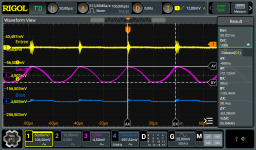
There I got a weird signal that was looking like a lot of oscillations. I had to stop this as the Power Supplys were becoming crazy toggling from one voltage to another. The transistor Q301, 302, 303, 401, 402 and Q403 was a bit hot to the fingers. I bet I blow them all!
I removed all the resistors in parallel and start over from scratch with 5 VDC. There I get this signal below that make me thing I burn them again. I have ordered a 100 of each 2N5401 and 2N5551. So I will replaced them and start again from scratch.
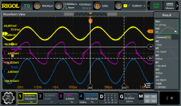
I replaced all six transistors above. This is one situation where you are happy to have chosen a 2 oz copper board! The old transistor were good from the tester. I still have this distortion on the BIAS, and when I removed the signal at the input, I still have a little signal at 26 kHz. See pictures below. I am now back at the beginning without any resistor across R104 nor R204. Back to 39 Ohms.
Attachments
H
HAYK
With 1k across R104 is enough for now because the opposite R204, the feedback will adjust itself with output offset. You deal with it after the outputs are enabled. Go back with single add resistor and adjust it to get 350mv to 400mv across R304. Now you said the opposite was 100mv more, this is not normal, measure the offset if in mv , check the driver transistors, one might be leaking.
Last edited by a moderator:
@HAYK, thanks so much for your patience and your step by step approach, I do appreciate it 😎
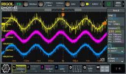
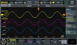
So I did start from the beginning. First, I measured the actual voltages with the original 39 Ohms for R104. In the capture below I configured my scope to always show the DC voltage at the output. That is the "DVM(C4)" to the right windows "Result". But I must admit that this scope is a fresh new product from Rigol and I have already found some bugs in it, even after having upgrade the firmware. The Bode Plot have problems with the channel 3 and 4, but that is another story. I already wrote to Rigol about it. But my doubts come from the 15,65 mV DC that the scope measure on channel 4. I do measure 0 VDC from my Rigol multi-meter and from another handset multi-meter.

So here are my measurements in that setup:
Then I soldered a 1 kOhms resistor in parallel to R104 :
Pictures... I don't remember what I did between the two below. I think I move down the input from 50 mV to 25 mV :


After this, I replaced the 1kOhms parallel resistor with a 820 Ohms one. I wasn't able to measure because I could hear high pitch tone from my computer speakers. That is weird, as if my coomputer audio pré-amp that drive two preamplifed speakers was getting noise at high frequency. And the Power Supplys became crazy again. I tried to stop the input signal to measure the voltage across R304 but when I put my multi-meter tip on the resistor pin, the positive Power Supply start to fall down it's voltage. And I use my handset multi-meter for this test to be sure I don't interfere with all the others gears.
So I stop everything and touch the transistor group Q301,302 and 303, and I burn my finger on them! The other group Q401, 402 and 403 were a bit hot but supportable.
I took this capture with only the input activate without any DC on the rails voltage, just to prove the input signal isn't that noisy.

So I did start from the beginning. First, I measured the actual voltages with the original 39 Ohms for R104. In the capture below I configured my scope to always show the DC voltage at the output. That is the "DVM(C4)" to the right windows "Result". But I must admit that this scope is a fresh new product from Rigol and I have already found some bugs in it, even after having upgrade the firmware. The Bode Plot have problems with the channel 3 and 4, but that is another story. I already wrote to Rigol about it. But my doubts come from the 15,65 mV DC that the scope measure on channel 4. I do measure 0 VDC from my Rigol multi-meter and from another handset multi-meter.
So here are my measurements in that setup:
R104 = 38,867 Ohms
OUTPUT = 0 VDC
R304 = 487 uVDC
Then I soldered a 1 kOhms resistor in parallel to R104 :
R104||1k Ohms = 37,394 Ohms
OUTPUT = 1,106 VDC
R304 = 281 mV
Pictures... I don't remember what I did between the two below. I think I move down the input from 50 mV to 25 mV :
After this, I replaced the 1kOhms parallel resistor with a 820 Ohms one. I wasn't able to measure because I could hear high pitch tone from my computer speakers. That is weird, as if my coomputer audio pré-amp that drive two preamplifed speakers was getting noise at high frequency. And the Power Supplys became crazy again. I tried to stop the input signal to measure the voltage across R304 but when I put my multi-meter tip on the resistor pin, the positive Power Supply start to fall down it's voltage. And I use my handset multi-meter for this test to be sure I don't interfere with all the others gears.
So I stop everything and touch the transistor group Q301,302 and 303, and I burn my finger on them! The other group Q401, 402 and 403 were a bit hot but supportable.
I took this capture with only the input activate without any DC on the rails voltage, just to prove the input signal isn't that noisy.
Attachments
@Sevy What is important for this topology to establish a predictable, reasonably stable VAS standing current is a degeneration resistor at the VAS transistor emitter, and that resistor is 0-ohm, or absence, in your schematic. The absence of that degeneration is the cause of you kept smoking transistors. Without the degeneration the compound transistor Q301-Q303 can pass a large enough current through Q301 collector-emitter and through Q303 b-e junction to blow them both. A few members' responses mentioned degeneration, but they seemed to have been overlooked.
The attached is a proposal to the improvement. The proposal aims at a VAS standing current about 8.5mA, and the Q301 emitter current not be much greater than 1mA.
1) Adding 47K resistor to shunt the current mirror, this resistor passes the mirror's reference voltage to the VAS stage. By the way this resistor should not be lower than about 4.7K in resistance or it would negate the merit of current mirror loading.
2) Adding R001 at Q303 emitter,
3) Adding D001 to bump the reference voltage at the input stage current mirror to 2x b-e junction drop plus the voltage drop at the current mirror degeneration resistor. By doing so the operating voltage across R001 would be about the same as the voltage across the current mirror degeneration resistor (R104).
4) Changing the resistor values as noted, 39 to 220, 100 to 1k,
5) Do the above to the bottom half. Note the diode negative always points downwards.
Many times it's perhaps more important to try to understand how a circuit not work than to understand how it does.
Well... I officially declare my board as a "Prototype" lol ;-)
@nattawa , I did your modifications proposal,... with good success! The reason why I didn't apply the degeneration suggestions before is simple. I didn't understand where in the schematic these suggestions were targeted. Don't judge my experience by my PCB design. I am a senior drafter but even if I am a certified technician, I am a novice to Power Amp. I made a drafting career so my knowledge of practical electronic is limited to the understanding of schematics and the recap and calibration of R2R and cassettes decks. Even if I read a lot of books, I didn't put them in practice, except maybe for my tube pre-amplifier projects and my RIAA tube pre-amplifier project, but that is another story.
When peoples take the time to refer their solution with the parts references of my schematics, you understand how easy the modifications became in my mind ;-)
Anyway... I got pretty good results with your design modifications. First I found the results limited, everything was stopping around 20 kHz. But after some rest, I remember that I had limited the current to 100 mA on my Power Supply from the beginning tests. Raising that to 200 mA I was able to reach 100 kHz!
@HAYK, with the above modifications, and with 150mV à 1 kHz into the input, I measured 619 mV across R304 et -618 mV across R404. You suggested 400 mV, so I guess the nest step would be to modify R104 to reach it. Am I right?
I insert some picture of the curves...
Attachments
-
 20231101_144056.jpg112.5 KB · Views: 83
 -
 20231101_144025.jpg101.2 KB · Views: 90
 -
 20231101_144010.jpg264.8 KB · Views: 84
 -
 20231101_144004.jpg232.1 KB · Views: 76
 -
 20231101_143950.jpg278.9 KB · Views: 85
 -
 20231101_143923.jpg349.5 KB · Views: 89
 -
 RigolDS0.png44.9 KB · Views: 86
 -
 RigolDS7.png51.9 KB · Views: 89
@Sevy Taking static operating condition measurements of a circuit should be done without signal input. If without signal input you still get 619mV it's a bit too far from calculation. And it means the VAS current is too high, at about 16mA, that the over-current protection has come into action to starve the VAS transistors.
The 8.5mA VAS standing current target in my proposal was based on this resistor R105 being guessed to be 180 ohm.

That was the best resolution and best guess I could make out from your schematic. Is it indeed 180 ohm? What is the voltage across it? what are the voltage readings over the "new" 220-ohm resistors?
The 8.5mA VAS standing current target in my proposal was based on this resistor R105 being guessed to be 180 ohm.
That was the best resolution and best guess I could make out from your schematic. Is it indeed 180 ohm? What is the voltage across it? what are the voltage readings over the "new" 220-ohm resistors?
Last edited:
Oh! I didn't realize that my schematic would have been made lower in resolution when I shared it. Yes the value of R105 is 180 Ohms. To recap my resistors values choices, I followed Slone book saying that all standard values in figure 11.14 were the same as those from figure 10.2 and all the variable ones was based on the final Power desired in Watts. So I made a spreadsheet that referred all parts references of both figures 10.2 and 11.14, and made a cross reference to my parts references because I prefer using my naming convention. Basically, parts references of the input stage are labelled starting from 100 for the upper side and from 200 for the lower side. The VAS parts references start from 300 for the upper side and 400 for the lower side. Idem for the OPS with 500 and 600 respectively. All others parts references that are common start from 1, 2, 3 etc.
It is much more easy for the mind to remember when looking at the PCB. You measure across R304, then R404 for the lower side. As a convenience for the tracking, here are two captures of the fixes and variables values of my spreadsheet with the cross references between the originals figures and my schematics. The grey columns are the originals values of the book. The white ones are my references values. I calculated the variables values for both a 40 Watts RMS Output with a +/- 25 VDC rails and two MOSFETs in parallel, with the liberty of using only one MOSFET or two MOSFETs for more power, as well as a 70 Watts RMS Ouput with a +/- 35 VDC rails. The latest also to compare my calculations with those of the book that were based for 70 Watts RMS.
P.S.: Now that I read back myself before posting, I realize that I shouldn't go over +/-25 VDC in my tests below because I have resistors values soldered for my 40 Watts RMS version with a +/- 25 VDC! I forgot this details design after all the time passed since my spreadsheet creation :-/


Now, back to your measures requests, I started at 5 VDC, and raised the rails step by step until 35 VDC, with no signal at the input. Here are the results:
Rails at +/-5 VDC:
Rails at +/-10 VDC:
Rails at +/-15 VDC:
Rails at +/-20 VDC:
Rails at +/-25 VDC:
Rails at +/-30 VDC:
At +/-35 VDC on the rails, I noticed that the positive Power Supply took a couples of seconds to reach it 35 VDC. At all the above values, the transistors Q301, 302, 303 and Q401, 402, 403 were all colds. But once the positive Power Supply reach is +35 VDC the group Q301, 302, 303 (the upper side) was to hot for my fingers. I stopped the Power Supply's right there.
Back from my revision reading, here are the voltages requested across the new 220 Ohms resistors R102, 104, 202, 204, and R105, 205 180 Ohms resistors with a +/-25 VDC rails:
R102 404mV
R104 404mV
R202 -414mV
R204 -414mV
R105 684mV
R205 -674mV
And I put the above measures into a little grid calculation to find the right resistors for getting around 8mA across R304 and R404. Am I correct with a 75 Ohms values for them?

It is much more easy for the mind to remember when looking at the PCB. You measure across R304, then R404 for the lower side. As a convenience for the tracking, here are two captures of the fixes and variables values of my spreadsheet with the cross references between the originals figures and my schematics. The grey columns are the originals values of the book. The white ones are my references values. I calculated the variables values for both a 40 Watts RMS Output with a +/- 25 VDC rails and two MOSFETs in parallel, with the liberty of using only one MOSFET or two MOSFETs for more power, as well as a 70 Watts RMS Ouput with a +/- 35 VDC rails. The latest also to compare my calculations with those of the book that were based for 70 Watts RMS.
P.S.: Now that I read back myself before posting, I realize that I shouldn't go over +/-25 VDC in my tests below because I have resistors values soldered for my 40 Watts RMS version with a +/- 25 VDC! I forgot this details design after all the time passed since my spreadsheet creation :-/
Now, back to your measures requests, I started at 5 VDC, and raised the rails step by step until 35 VDC, with no signal at the input. Here are the results:
Rails at +/-5 VDC:
R304 442mV
R404 -443mV
Rails at +/-10 VDC:
R304 536mV
R404 -537mV
Rails at +/-15 VDC:
R304 587mV
R404 -586mV
Rails at +/-20 VDC:
R304 616mV
R404 -615mV
Rails at +/-25 VDC:
R304 634mV
R404 -634mV
Rails at +/-30 VDC:
R304 643mV
R404 -643mV
At +/-35 VDC on the rails, I noticed that the positive Power Supply took a couples of seconds to reach it 35 VDC. At all the above values, the transistors Q301, 302, 303 and Q401, 402, 403 were all colds. But once the positive Power Supply reach is +35 VDC the group Q301, 302, 303 (the upper side) was to hot for my fingers. I stopped the Power Supply's right there.
Back from my revision reading, here are the voltages requested across the new 220 Ohms resistors R102, 104, 202, 204, and R105, 205 180 Ohms resistors with a +/-25 VDC rails:
R102 404mV
R104 404mV
R202 -414mV
R204 -414mV
R105 684mV
R205 -674mV
And I put the above measures into a little grid calculation to find the right resistors for getting around 8mA across R304 and R404. Am I correct with a 75 Ohms values for them?
none of them should be even lukewarm, even at +/-50V rails. Something is broken. Check all transistors and diodes to the right of C102/202, out of circuit.the group Q301, 302, 303 (the upper side) was to hot for my fingers.
I don't know what you're trying to do with that chart, but R304/404 do not decide VAS current. They decide the overcurrent protection threshold. Their value should be set according to the VAS current of choice so that they have a voltage drop of about 300mV at that choice of VAS current.And I put the above measures into a little grid calculation to find the right resistors for getting around 8mA across R304 and R404. Am I correct with a 75 Ohms values for them?
What is the R303/403 values on the board now? I don't seem to see a 1Kohm resistor in your recent pictures.
Back from my revision reading, here are the voltages requested across the new 220 Ohms resistors R102, 104, 202, 204, and R105, 205 180 Ohms resistors with a +/-25 VDC rails:
R102 404mV
R104 404mV
R202 -414mV
R204 -414mV
R105 684mV
R205 -674mV
These readings are quite close to what I anticipated. They seem to suggest the input stage diff-pairs, their current mirror loading, and the tail current source are operating at the condition as intended....that means all things to the left of C102/202 work.
The circuit was designed to operate at minimum +/-15V rail voltages or thereabout. You can skip some of the many incremental steps and start at +/-25V rails, or simply go straight to +/-35V.
I am trying to understand better how everything work. In recent posts from HAYK, he was curious of the voltage across these resistors.I don't know what you're trying to do with that chart, but R304/404 do not decide VAS current. They decide the overcurrent protection threshold. Their value should be set according to the VAS current of choice so that they have a voltage drop of about 300mV at that choice of VAS current.
What is the R303/403 values on the board now? I don't seem to see a 1Kohm resistor in your recent pictures.
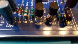
Resistors R303 and R403 are 1kOhms. They were originaly 100 Ohms but I replaced them based on your proposal in post #43. Although when I measured them on board, R303 is 0,982 kOhms but R403 is 0,977 kOhms.
This is a huge job. This morning I did a Bode Plot from 10 Hz to 100 kHz with +/-5 VDC rails and a 20 mV signal. Can this remove any doubth about a possible bad part?Check all transistors and diodes to the right of C102/202, out of circuit.
Are you talking all parts in the VAS only or also in the OPS?
I got two goods news and one bad news.
- I received my book "Desiging Audio Power Amplifiers, Second Edition - Bob Cordell
- I created a new version "Rev1.1" of my design with the modifications proposed my nattawa in post #42, and the PCB is ready for production, after this one will be fully functional first!
- After my DHO914S bugs reports to Rigol, they concluded that my scope is defective and proposed me a new replacement at no charge. Even if this look like a good news, I may have to send mine first before they send me the new one. This could take 2 weeks from their evaluation and I don't have another scope in the mean time :-[ That is shocking!
No point doing any performance tests to a broken circuit that burns your finger.This morning I did a Bode Plot from 10 Hz to 100 kHz with +/-5 VDC rails and a 20 mV signal.
A necessary job is never too huge I'm afraid. At least not as huge as posting a clearly legible schematic, eh?😊This is a huge job.
PCB can wait. That proposal was just the first steps towards the right direction. There is one more major bug in your schematic that can lead to function failure and/or device damages.I created a new version "Rev1.1" of my design with the modifications proposed my nattawa in post #42, and the PCB is ready for production,
The over-current protection to the VAS is at the wrong place.
It is clear to see that when the current going through R304 approaches about 15mA, Q302 starts to turn on and limit that current by bleeding off the base drive at the cascode transistor Q304. However, there is nothing that circuit can do to stop Q301 dumping a significant current through the base junction of Q303, smoking itself and Q303 as well in the event the amp is over driven into clipping, or devices in other areas fail and make the overall feedback loop going open-loop -- of which the latter case was my speculation and why I suggested a health check to the semiconductor devices as I did.
The solution is a re-designed VAS protection as attached. You can find that exact protection topology and description in Bob's book you've just received.

New status...
Last week I wasn't that happy with the Rigol proposal seeing that I would have been without a scope for at least two weeks. Even if their solution was totally free, I choose to communicate my frustration with the provider of the scope; Electro-Meters. I bought it on September 13, 2023. Then one agent personally call me to explain the delay on this product. She send me a first email to confirm that Electro-Meters had a ship date of 10/16/23. Then a second email that says a new shipping date on 10/20/2023! Finally a good news saying a shipping from UPS on 10/17/2023. I received it at home on 10/18/2023, more than a whole month of waiting!
So I write her back last Friday explaining her my situation and asking her what kind of warranty Electro-Meters could honor in such a situation. I even tell her that I would be open to buy a new item and on it's receive, I would have send back the defect one for a refund. The first answer I received was a purchase order for a new scope with an amount of 0,00 $!!
After a couple of emails, I understood that they agreed to send me a new scope for free the same day (that's last Friday) and that I would receive it on Monday (today). And they let me know that I could send back the bad one at my convenience. I do cross my fingers now in the hope that this new one will be without any bugs.
I do write this story because I want to share with every readers that this company is a very understanding one and that they satisfy me totally. On this days, it is rare to have such a good service. Of course I will have to pay for the shipping of the bad one but I prefer that instead of two weeks of waiting.
As for the book, I guess none are perfect! I am the kind of guy who find mistake without any effort. It is like this at my job to. I simply read a text and, don't ask me why, my eyes always sees the typing errors. I am starting to thing that it's a gift from God (lol).
So reading the book I already saw errors in it that I will probably share to the author on it's website. For example, on page 77 Figure 3.13, there are three occurrence of Q14 in the schematic. Page 80 Figure 3.14, the author explain in the preceding pages that the value of all the RE resistors from the preceding schematic have been changed from 0.33 Ohms to 0.22 Ohms in this one. But the schematic still have 0.33 Ohms in it. But I am not here to complain, just to share to everyone to stay attentive.
Now back to the circuit... and to answer nattawa, I created the new PCB design with all the modifications until now just to take some advance for the future. I understand that it is not totally debugged but I had time to do it and I wanted to see what would be the physical impact of those modifications on my actual design. Would I have enough space to insert them? It was easy to copy the whole project to Rev1.1 and apply the PCB modification from the schematic net-list.
Also, yesterday I removed all the diodes and transistors on the VAS stage to test them outside as you suggested in post #52. They were all testing good but having ordered a bunch of 2N5551, 2N5401 and 4.4 VDC Zener diode (100 each) I did replaced them with new one. I did also replace the 2SB649 and 2SD669 with new one. And today I will remove totally the two MOSFETs, even if their drain are out of the circuit as HAYK suggested me in post #7, from the book testing procedure I think it will be safer to simply remove them before any new tests.
I studied your latest modifications in post #55. The 47K balancing resistors and the 1N4148 diodes modifications in the IPS are already made on my PCBs since your post #48. As for the VAS modifications, you will find below two screenshots. the first one is the actual situation since your post #48 and the right one is my understanding of your latest proposal applied to my schematic. Before I do the hardware modification, could you confirm me that it is as you suggest?
ACTUAL SITUATION

NEW PROPOSAL

Thanks!! 🙂
EDIT: The pre-drivers Q502 and Q602 have also been replaced with new one...
Last week I wasn't that happy with the Rigol proposal seeing that I would have been without a scope for at least two weeks. Even if their solution was totally free, I choose to communicate my frustration with the provider of the scope; Electro-Meters. I bought it on September 13, 2023. Then one agent personally call me to explain the delay on this product. She send me a first email to confirm that Electro-Meters had a ship date of 10/16/23. Then a second email that says a new shipping date on 10/20/2023! Finally a good news saying a shipping from UPS on 10/17/2023. I received it at home on 10/18/2023, more than a whole month of waiting!
So I write her back last Friday explaining her my situation and asking her what kind of warranty Electro-Meters could honor in such a situation. I even tell her that I would be open to buy a new item and on it's receive, I would have send back the defect one for a refund. The first answer I received was a purchase order for a new scope with an amount of 0,00 $!!
After a couple of emails, I understood that they agreed to send me a new scope for free the same day (that's last Friday) and that I would receive it on Monday (today). And they let me know that I could send back the bad one at my convenience. I do cross my fingers now in the hope that this new one will be without any bugs.
I do write this story because I want to share with every readers that this company is a very understanding one and that they satisfy me totally. On this days, it is rare to have such a good service. Of course I will have to pay for the shipping of the bad one but I prefer that instead of two weeks of waiting.
As for the book, I guess none are perfect! I am the kind of guy who find mistake without any effort. It is like this at my job to. I simply read a text and, don't ask me why, my eyes always sees the typing errors. I am starting to thing that it's a gift from God (lol).
So reading the book I already saw errors in it that I will probably share to the author on it's website. For example, on page 77 Figure 3.13, there are three occurrence of Q14 in the schematic. Page 80 Figure 3.14, the author explain in the preceding pages that the value of all the RE resistors from the preceding schematic have been changed from 0.33 Ohms to 0.22 Ohms in this one. But the schematic still have 0.33 Ohms in it. But I am not here to complain, just to share to everyone to stay attentive.
Now back to the circuit... and to answer nattawa, I created the new PCB design with all the modifications until now just to take some advance for the future. I understand that it is not totally debugged but I had time to do it and I wanted to see what would be the physical impact of those modifications on my actual design. Would I have enough space to insert them? It was easy to copy the whole project to Rev1.1 and apply the PCB modification from the schematic net-list.
Also, yesterday I removed all the diodes and transistors on the VAS stage to test them outside as you suggested in post #52. They were all testing good but having ordered a bunch of 2N5551, 2N5401 and 4.4 VDC Zener diode (100 each) I did replaced them with new one. I did also replace the 2SB649 and 2SD669 with new one. And today I will remove totally the two MOSFETs, even if their drain are out of the circuit as HAYK suggested me in post #7, from the book testing procedure I think it will be safer to simply remove them before any new tests.
I studied your latest modifications in post #55. The 47K balancing resistors and the 1N4148 diodes modifications in the IPS are already made on my PCBs since your post #48. As for the VAS modifications, you will find below two screenshots. the first one is the actual situation since your post #48 and the right one is my understanding of your latest proposal applied to my schematic. Before I do the hardware modification, could you confirm me that it is as you suggest?
ACTUAL SITUATION
NEW PROPOSAL
Thanks!! 🙂
EDIT: The pre-drivers Q502 and Q602 have also been replaced with new one...
Last edited:
Confirmed.could you confirm me that it is as you suggest?
There are a few spots that you probably can put in options/changes.
1. R301 (the other resistor in bottom half as well) is tied to power rails at present, an option could be provided in the PCB layout so that both are tied to Vout instead. This allows experimenting switching the compensation scheme between TPC (Two-Pole Compensation) and TMC (Transitional Miller Compensation). The latter in general offers a smoother loop gain response and a slightly better stability margins. Bob's book has the discussion.

2. 2SB649/D669. These are slow devices with Ft at mere 1MHz, they (except non-critical Q1) could be replaced with TTA004/TTC004 that have Ft goes far out to 100MHz, for better expected performance and stability. They are package compatible devices -- drop-in replacement.
3. If it matters, the 4.4V zener D301 eats a bit too much into the signal headroom. 2.7V is all it needs. They could be a LED with forward voltage at 2.7-3.0V.
Last edited:
How many times? I'joking, of course🙂!!! Sevy, do yourself a favor, make your life easier - changed the book, changed the circuit, changed the scope etc.So I did start from the beginning.
My humble suggestion is:
-author: G. Randy Slone
-book: ''THE AUDIOPHILE'S PROJECT SOURCEBOOK'' 80 high-performance audio electronics projects
-chapter: six/6/- ''Audio Power Amplifiers''
-pages: 172, 173, 174, 175, 176,177, 178179, 180, 181, 182, 183
-figure: 6-21/page 173/
-PCB: pages 179, 180, 181
This is a tested, working circuit and PCB. Recommended by friends, approved, despite neighbors' anger. Quite seriously. Just one more thing:
https://ptodorov.com/a-solid-state-tale-my-favourite-amp/
I don't know the man, just FYI.
? Not exactly - 140 MHz.2. 2SB649/D669. These are slow devices with Ft at mere 1MHz,
Yes, you're right. My mistake. Please disregard that part of my comment. However, if B649/D669 are hard to source, TTA004/TTC004 are good alternative.? Not exactly - 140 MHz.
- Home
- Amplifiers
- Solid State
- Need helps! Weird signal results on my DIY High-performance Hyrid MOSFET Audio Power Amplifier