In the real amp this is the resistor that is being driven (last image). In the simulation we add it as a load. So whatever value that resistor is in the real amp you can then add to the sim.
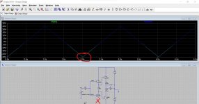
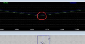
Run the sim and look at Vin and Vbase. The two traces overlap because the voltage is the same on each end of the 10k.
Now cut the collector of the driver transistor and run it again. Zoom in on the lower tip of the waveform and you will see the voltage difference separating them. That voltage difference is across the 10k. Vbase is lower than Vin because the stage is now loading the driving voltage source because it has low current gain because of the 'damaged' transistor.
Got to disappear again 🙂
Attachments

can these packs be renewed/replicated? i know they are old but there must be an equivelent?
A Vbe multiplier would be the best solution. The economy version 😀 which is just as good as a full version but uses less parts consists on one transistor and one preset.
Later...
The diode pack version of the amp runs at fixed bias so you need to be careful when reinstating this. Use the bulb tester and do just one channel and check if it is OK.
If it is OK then I would link the pack out again before testing the second channel. Doing that allows the rails to be as high as possible with the bulb.
Remember, if the diode packs have a problem or are intermittent then the bias current could suddenly shoot very high (destructively so) although the bulb would limit current.
Before you do any of that you can test the amp with music. If there is a low gain situation in the output stage then this might reveal it. The amp should all work OK with no bias current. There might be a bit of audible distortion at low volume but a problem with the output stage would show at higher levels.
If for example the PNP driver transistor is open circuit on its collector (or even the same for the PNP output transistor) then the amp would still work and would be able to produce a couple of watts of audio before it ran into trouble.
ah it just clicked what you said about the idle current, this still needs to be adjusted then as it should be between 10 and 20mv, not 0v and they are both exactly 0v, i find this a bit odd dont you that they would both be exactly 0?
i dont think i will plug it into speakers just yet.
i dont trust this at the moment
so the current across R627 was 0mv
using the scale provided it said put a 1k resistor in parellel if the reading is between 0.4 and 0.8mv, well it wasnt even 0.4 but i tried a 1k and its still 0v
this theroreticaly should have made it somewhere near 10mv
so i tried a 4k one and no difference so something isnt right
im going to try the good channel and see if that is any difference, but it doesnt seem right to me.
what would be the effect of shorting out R637 and R629? (by mistake i mean ) it did spark a bit and now the lamps on again 🙁
ah it just clicked what you said about the idle current, this still needs to be adjusted then as it should be between 10 and 20mv, not 0v and they are both exactly 0v, i find this a bit odd dont you that they would both be exactly 0?
i dont think i will plug it into speakers just yet.
It gets very confusing. All I have for the 3030 is the diagram. Idle current is measured in milliamps but may be quoted as a voltage across a resistor.
i dont trust this at the moment
so the current across R627 was 0mv
using the scale provided it said put a 1k resistor in parellel if the reading is between 0.4 and 0.8mv, well it wasnt even 0.4 but i tried a 1k and its still 0v
this theroreticaly should have made it somewhere near 10mv
so i tried a 4k one and no difference so something isnt right
im going to try the good channel and see if that is any difference, but it doesnt seem right to me.
R627 on my diagram is the 6k8 between the base of the driver transistors. The voltage across this resistor is always going to be in the 2.5 volt region. If the diode pack is linked out then it would be zero of course.
what would be the effect of shorting out R637 and R629? (by mistake i mean ) it did spark a bit and now the lamps on again 🙁
Shorted to what? One resistor to the other or each one to ground. For R629 it would depend which end got shorted. If the bulb is on all the time then you probably zapped one or more of those four transistors.
im defending myself with this one 😉
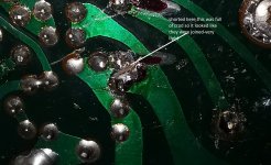
Lots of flux can make it hard to see what is underneath 🙂 It happens.
It gets very confusing. All I have for the 3030 is the diagram. Idle current is measured in milliamps but may be quoted as a voltage across a resistor.
R627 on my diagram is the 6k8 between the base of the driver transistors. The voltage across this resistor is always going to be in the 2.5 volt region. If the diode pack is linked out then it would be zero of course.
Shorted to what? One resistor to the other or each one to ground. For R629 it would depend which end got shorted. If the bulb is on all the time then you probably zapped one or more of those four transistors.
just between those 2 resistors
Lots of flux can make it hard to see what is underneath 🙂 It happens.
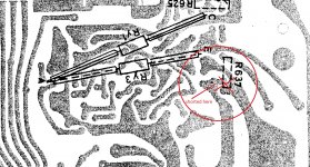
here you go
Thanks. OK, so that makes sense 🙂 It was R637, not R627. I thought it sounded wrong 😀
You will have to see how it works out when you are happy it is all otherwise OK. I'm not a fan of fixed bias designs like this as they are so critical on the actual parts used. Even minor differences in replacements can bring the adjustment out of range... but we will see.
R637 is so low in value that it won't matter which end you shorted on that one (but check it is OK and not open circuit. It should OK as the bulb should have saved it).
If it touched R629 on the -30 volt side then you shorted the output to the negative rail. That probably zapped the upper NPN output and maybe the driver.
If it touched the other side of R629 then I think it might have burned R629 up and also damaged other parts round Q605 and Q607.
If it sparked it was probably the supply side it touched so just output and driver suspect.
Remember, link the diode pack out and the output stage should draw no current.
im proberbly going to change the transistoras any(not the output they are ok) but none of the others are of original spec, Q 607 for example ,a BD139, isnt what is fitted, but it is what i put back.
ill just plod through it untill i get it sorted.
Before i shorted out those 2 resistors, the thing that is bothering me more than anything is this idle,its just at zero, no matter what i put across R625/6
maybe other components around the board have failed, caps or resistors low in value or shorted.
The idle current should be easy to diagnose if a little tricky to resolve. Just follow the theory...
The diode pack should have about 2.5 volts across it (four diodes in series). That 2.5v should be enough to just start to turn on the four transistors. You have 2.5 volts divided by four giving 0.625 volts. So that is each transistors share if they are all equal. That 0.625 volts will appear across each B-E junction.
If that is happening and all the transistors are good then you have just found the limitations of 'fixed bias' which is that it is much to design dependent and relies on the exact transistor types used by NAD. If that happens you need to modify the circuit to give a little more voltage across the diode pack. One option is to add a low vale resistor in series with the pack.
Current is about 10 milliamps so something like a 10 ohm would add another 0.1 volt to the total. It really will be this critical. You then go up in steps until the correct bias point is reached.
If you find you can not get any bias current at all even with higher voltage across the pack + resistor chain then you still have an output stage fault.
Speaking of the mess and a NAD, I am now trying to figure out what is wrong with NAD 310 amp. One channel is fine, the other has full voltage in the middle junction, just at the ouput capacitor (it should be half voltage). The problem is, there is a ghost in the machine! Even though all semiconductors measure fine, and almost all el. Capacitors have been replaced, I haven't found the source of failure yet! So, maybe I will open another NAD in a mess thread...
what is the difference between 2 transistors that are the same spec but one is -65v rated and the other is 65v rated? how would i know which one to buy?The idle current should be easy to diagnose if a little tricky to resolve. Just follow the theory...
The diode pack should have about 2.5 volts across it (four diodes in series). That 2.5v should be enough to just start to turn on the four transistors. You have 2.5 volts divided by four giving 0.625 volts. So that is each transistors share if they are all equal. That 0.625 volts will appear across each B-E junction.
If that is happening and all the transistors are good then you have just found the limitations of 'fixed bias' which is that it is much to design dependent and relies on the exact transistor types used by NAD. If that happens you need to modify the circuit to give a little more voltage across the diode pack. One option is to add a low vale resistor in series with the pack.
Current is about 10 milliamps so something like a 10 ohm would add another 0.1 volt to the total. It really will be this critical. You then go up in steps until the correct bias point is reached.
If you find you can not get any bias current at all even with higher voltage across the pack + resistor chain then you still have an output stage fault.
Speaking of the mess and a NAD, I am now trying to figure out what is wrong with NAD 310 amp. One channel is fine, the other has full voltage in the middle junction, just at the ouput capacitor (it should be half voltage). The problem is, there is a ghost in the machine! Even though all semiconductors measure fine, and almost all el. Capacitors have been replaced, I haven't found the source of failure yet! So, maybe I will open another NAD in a mess thread...
A new thread is best tbh 🙂 this one is super specific... and with a good title 😉
what is the difference between 2 transistors that are the same spec but one is -65v rated and the other is 65v rated? how would i know which one to buy?
You might find PNP devices marked with negative voltages in some spec sheets because the collector is always negative with respect to the emitter on these. Some show them like this and some don't.
Its like specifying a fuse to be used in a negative rail as a -3 amp fuse. Its meaningless but technically correct.
- Home
- Amplifiers
- Solid State
- NAD 3030 in a mess