I spent a few minutes playing around with the layout to make some quick and dirty changes to the track routing:
Added some curved traces to give it a 1970's look.
From the images you should be able to make the changes to your local Kicad files.


- Rotate Q401 anticlockwise
- Rotate Q407 clockwise
- Rotate C424 clockwise
- Aligned R411 and C417 so pads are inline with R413
- Rotate R431 anticlockwise
- Rotate R433 clockwise
- Move C421 down a bit
- Move R423 up a bit
- Rotate R407 clockwise
- Aligned C401 and R401 to the pads of R405
- Aligned R417 to C405
From the images you should be able to make the changes to your local Kicad files.

Tried that but it still comes up with the disconnected error. I'll try againThey look like errors where you have unconnected track segments.
Either use the track connection 'tool' that's listed somewhere on the top menus, or just delete both track segments and redraw as a single track.
Look at your first error: 'missing connection Net Q407-B'.
You've drawn track(s) between R425 & C413, but not connected them to Q407-B. Kicad is showing you the ratsnest link from C413 to Q407-B... connect that and it'll probably be sorted.
You've drawn track(s) between R425 & C413, but not connected them to Q407-B. Kicad is showing you the ratsnest link from C413 to Q407-B... connect that and it'll probably be sorted.
Not sure whats happened here as the rats nest wants to go over the other side now and a load of faults have shown up

seems to be going from bad to worse for some reason.I correct an error then aload more come up after-a bit frustrating
Not sure whats going on here.I correct faults then it just gives me a load more 'does not match copy in library?? ive already taken this resistor out on the scheme and replaced it but it still comes back the same, so i give up.
The reason for the error for JP1 is that it appears to have been modified the two pads are one footprint, it looks like the pads have been separated so it throws the error that its different.
Change JP1 on the schematic and add two pads and move them to the respective locations on the pcb.
Add "GND" symbols to your schematic.
You may have to increase the text sizes on the pcb to match the design rules of the pcb manufacturer.
Ensure the design rules in the pcb board setup meet the design rules of the pcb manufacturer.
It makes routing a little easier if you set the grid to 0.1000mm.
The ground plane on the bottom layer is missing.
I suggest you make changes to the layout as per post #281.
I fixed most of the errors, you just need to replace JP1 with some pads and add the ground plane back to the bottom layer.
Attachments
seems to be going from bad to worse for some reason.I correct an error then aload more come up after-a bit frustrating
I have no idea what you're doing now - and I won't have Kicad access for most of the next month, so attached is your layout, as you posted in #273, but corrected for everything except the transistor sizes. I strongly suggest to correct those still (they will be a nightmare to hand-solder as they are) - but only do one at a time, and make sure it's correct before moving on to the next.
I see 'Indiglo' has already replied while I was typing (thanks 👍) - so feel free to follow his suggestions instead and/or as well, I'm sure they're good.
Attachments
not sure how the ground plane has gone, it was there.Bit confused about the 'JP1' bit as this was how goldie showed me to do it and it was ok.The reason for the error for JP1 is that it appears to have been modified the two pads are one footprint, it looks like the pads have been separated so it throws the error that its different.
Change JP1 on the schematic and add two pads and move them to the respective locations on the pcb.
Add "GND" symbols to your schematic.
You may have to increase the text sizes on the pcb to match the design rules of the pcb manufacturer.
Ensure the design rules in the pcb board setup meet the design rules of the pcb manufacturer.
It makes routing a little easier if you set the grid to 0.1000mm.
The ground plane on the bottom layer is missing.
I suggest you make changes to the layout as per post #281.
I fixed most of the errors, you just need to replace JP1 with some pads and add the ground plane back to the bottom layer.
I recon this is pretty good now.Ive changed the footprints of the transistors/resistor and capacitors where they were a bit small and tidied it up.

Some of the improvements suggested by Indiglo would help 'tidy' the board a bit more, but otherwise (and provided you've already input all the JLCPCB requirements I gave you before) from a JLCPCB production perspective it should work. The remaining JP1 error is irrelevant for the Gerbers as far as I know (you'll be fitting a free wire link, so the exact geometry of the 2 pads is less relevant).
I did all the JLCPBC stuff a while ago, so i guess thats it, im not going to mess about with it anymore
so is there anything else i need to do with this.How do i go about getting it made?
I obviously need 2 of these, so do i need to do the whole thing again from scratch for the other board or can it be duplicated/copied with the other boards references?
I obviously need 2 of these, so do i need to do the whole thing again from scratch for the other board or can it be duplicated/copied with the other boards references?
As I've already told you, I'm now travelling, with no access to Kicad - but in any case, I have already answered all of these questions. If you can't be bothered to take notice of information I've already provided, then I'm afraid I will no longer be repeating myself.
All good and have placed the order, so once they arrive ill update 👍I'll be travelling quite a bit in the next few weeks, with only occassional access to Kicad, so to round this off - the instructions for completing & ordering the pcbs.
Once the final DRC checks are good - plotting the Gerbers is very straightforward:
On the pcb screen - go to 'File' - 'Plot' - then select 'Plot Format' = Gerbers, and give it a directory to put them in (or leave blank to put them with the rest of the Kicad Project files).
Once that's done, check the tick boxes in the first column ('Include Layers') - you need to tick any and every layer that you've used for the pcb,
then check the 'Plot on all layers' column - they should all be unticked. Finally, check the other general options are as follows, and then press 'Plot'
View attachment 1438607
Let 'Plot' do it's thing, then, while you're on the same screen, press the 'Generate Drill Files' button. That'll open a new screen, leave everything set to the default values, and just press 'Generate Drill File'.
Again, let it do it's thing, then press 'Close' (2X), to return to the pcb screen.
You should now have all of the required Gerber & Drill files listed in the main Kicad project screen (where the pcb, schematic, and back-up files are all kept).
Those are the files needed by JLCPCB (all files with file type .gbr or .gbrjob or .drl, nothing else). Zip all those files together into one compressed zip file/folder and you're ready to place an order at JLCPCB
https://jlcpcb.com/
There's an "Add Gerber File" box on the home screen at JLCPCB, just click that and select the zipped Gerber file on your pc. The JLCPCB site will upload it, and should show you a front & back view of the pcb, with a bunch of production options to choose from, as well as a preliminary price indication (I just uploaded a copy to double check the instructions).
View attachment 1438993
You can basically leave everything on the default values for this pcb, although you could obviously change colours etc. if you want. The key parts are FR-4, 1.6mm pcb thickness, 2-layer, 1oz Copper, HASL (with or without Lead - I go 'with'), and the number of pcb's you want (5X is the minimum). When you've set the options you want, the price is already shown. Just press 'Save to Cart' to add the pcb project to the shopping cart. Shipping costs are added when you complete the order, I normally just use the cheapest and have never had a problem (takes up to ca. 2 weeks to UK).
Once the order is placed, JLCPCB will audit everything to ensure it suits their production parameters, and it'll be produced typically within 1 - 3 days. It is possible it'll fail the audit but unlikely if you've set the various parameters as I've listed throughout this thread and if it passes the DRC checks in Kicad. There's no charge if it does fail, you can either correct or cancel the order.
One extra point:
The schematic & pcb as they are currently are for the R-Channel phono amp. The left channel is identical but uses all even numbered part references. To produce unique R-Ch and L-Ch pcb's, the simplest would be to copy the entire R-Channel project, re-number the parts on the copied schematic & pcb. You could add simple text boxes to the Front or Back silks to indicate L or R. You'd need to order the R and L pcb's as 2 separate projects at JLCPCB.
Anyway, hope that helps. Good luck.
so i eventualy have got round to dry fitting, and it fits without issue and everything lines up.
Only problem is at the moment i only have the right channel, and i can do as goldie suggests to do the left.But that means buying another 5 units, the min was 5.
so if i do the left channel i will have 4 of each channels left over spare, and im not sure what i would do with them.
so do i just use 2 of the rights? or do i do the left as suggested.
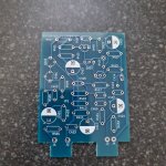
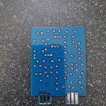
First one finished.
Few lessons learned with this.I could have gone a bit smaller with the caps as suggested by others, but im generaly quite pleased with my first attempt, so thanks to all who suggested and helped, especialy @Goldie99 , who put up with me through this process 👍
Few lessons learned with this.I could have gone a bit smaller with the caps as suggested by others, but im generaly quite pleased with my first attempt, so thanks to all who suggested and helped, especialy @Goldie99 , who put up with me through this process 👍
Attachments

Last edited:
- Home
- Amplifiers
- Solid State
- NAD 3030 complete rebuild