
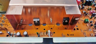
@Mooly @Goldie99
remember the NAD 3020 i converted to FETS with the copper heatsink.
I wonder how much work it would be to reproduce that board so that the FETS fitted striaght in, drivers removed etc
I had to cross over all the connections underneath.But i could make a board where everything just fits in.
remember the NAD 3020 i converted to FETS with the copper heatsink.
I wonder how much work it would be to reproduce that board so that the FETS fitted striaght in, drivers removed etc
I had to cross over all the connections underneath.But i could make a board where everything just fits in.
Attachments

Last edited:
Turn the 'model bounding boxes off (to see what you're doing), then adjust the 4X J pads as described (back in the pcb view).
If you zoom in on 3d view you can see where your B.Mask zones are removing the solder mask up to the edge of the pcb.
If you zoom in on 3d view you can see where your B.Mask zones are removing the solder mask up to the edge of the pcb.
Far more than it's worth, and also much more expensive - you'd be better off producing a 'protection' pcb, to correct one of the 3020 weaknesses.I wonder how much work it would be to reproduce that board so that the FETS fitted striaght in, drivers removed etc
remember the NAD 3020 i converted to FETS with the copper heatsink.
I wonder how much work it would be to reproduce that board so that the FETS fitted striaght in, drivers removed etc
It is a lot of work. You would have to copy the layout which means drawing it 'freehand' in KiCad (or whatever package you would use) making the required circuit alterations in the process. Its a non starter imo. The enthusiasm is good but you have to be realistic 🙂
You have to remember how the pcb interfaces (slots in) to the main NAD pcb - so your J3 & J4 silkscreen labels will not be visible like that. Howeve, since they serve no constructive purpose as 'J' numbers, I'd just change them to something meaningful, and put them on the visible pcb area - you can put them horizontal / vertical / wherever suits best. You can also add 'free' text wherever you want, e.g., add your own pcb reference (so it can be traced back to your files in future)... etc.
You can position the silkscreen items, e.g., part references, free text, etc., largely wherever you want on both the top or bottom silkscreen layers, as long as it doesn't impinge on any purple part 'courtyards'.

You can position the silkscreen items, e.g., part references, free text, etc., largely wherever you want on both the top or bottom silkscreen layers, as long as it doesn't impinge on any purple part 'courtyards'.
Pretty much done with this.Im not going to change the resistor footprints, i think they will be fine as they are

Fix the case and then test the transformer. It may be possible to put in a TPA3255 D Amp and have 125w.
The face is very nice.
The wood case may need to be rebuilt as well.
The face is very nice.
The wood case may need to be rebuilt as well.
@stocktrader200 , thanks for your comments.I already did all the case etc see post #20 onwards
thanks
thanks
It's not possible to properly 'review' your present design from just a snap-shot picture; you'd need to post the Kicad Project+Schematic+PCB fiels as a zip file for anyone else to be able to see the details.Pretty much done with this.Im not going to change the resistor footprints, i think they will be fine as they are
Based on what I can see:
# I think the connection tabs at the bottom are probably good now, but 'J5' & 'J7' seem to have wandered off - it maybe not an issue, but, as they are, they'll give 2 extra 'through-holes' on the pcb. As they're both GND 'connections', I just removed them, and added 'GND' labels to the B.Silk layer (depending on your schematic, you may need to remove them there as well).
# Your 'C403' reference on the F.Silk is way too small - you can change, move and rotate text on the silk layers largely at will, provided it still complies with the (DRC) production constraints that I posted back in Post #217.
# In terms of part sizes, R429 looks odd, but I can't see what's going on with it. Otherwise, you'll probably get away with the resistor footprints, but the transistor footprints you're using will almost certainly be an issue - not for JLCPCB, but for you to solder:
If you look at the physical size of the footprints you have at the moment, you'd need to hand solder 3x joints in the space of 2.5mm... that'd be fun even on a good day.

I'd suggest, it's a lot easier to just revise them to a more convenient footprint, e.g., "Package_TO_SOT_THT:TO-92L_Inline_Wide", that'll give you a much more realistic 5mm to work with.

To change them: Select a transistor on the pcb, double-click it to open its' properties page, then use the 'Change Footprint' option on the bottom right of the page to select the change footprint menu. Once that's done, just delete and redraw the 3 tracks to the transistor (one at a time is less confusing). It shouldn't take more than a minute or so per transistor.
Finally - everything will need to pass the Design Rules Checker (DRC), or it'll be automatically rejected by JLCPCB (been there, done that...). It'll probably be like previously, with lots of errors, but many will be very simple corrections - not one at a time. Once it's at that point and 'passes', it's only 2-3 minutes wotk to plot the relevant Gerber files and zip them for online submission to JLCPCB.
"Isolated copper fill not connected" - means you haven't set the properties of the J pads properly - double click on the yellow part of J3 say, that'll open the pad properties page (and it should be showing the "Connections" tab). Where it says "From Parent Footprint", change that to "solid", and click OK. Refill the zones and that pad should be OK. Do the same for the others.
Most of the other warnings are for text heights, sizes, thicknesses, and positions - just set the heights, thicknesses, etc. via the main Edit menu ("Edit text & Graphics Properties") or one by one (double click any reference text on the pcb view and it's properties page should open). Reposition any that are too close to purple courtyards (just drag & drop). Actually, you have an error in the 'Board Set-up" settings - go to File - Board Set-up - and change Text Thickness to 0.153mm - OK
The JP1 jumper footprint is screwed up - I'll have to look at that.
Edit: - and just delete the J5 & J7 pins - they're not needed once the connection zones are set up.
- and ignore the DRC warning for JP1 - that's just because it was edited on the pcb and not in the footprint library, it won't affect the Gerbers at all.
Last edited:
Not sure how you "update the pcb", but it looks as if you're updatng it for changes to the schematic (?). If that's the case, it'll always change JP1 to the jumper footprint that you've assigned on the schematic.
The JP1 footprint you were using in yesterdays file was fine...

If you make the corrections I indicated in #275, then run DRC - you should see this screen - with only 1 remaining DRC 'warning', that as far as I know you can ignore (it just means your pcb edited JP1 footprint is different to the library footprint).

At that point (and if you ignore all the previous warnings re. part sizes !) - it's ready to plot the final Gerber files needed for JLCPCB.
The JP1 footprint you were using in yesterdays file was fine...
If you make the corrections I indicated in #275, then run DRC - you should see this screen - with only 1 remaining DRC 'warning', that as far as I know you can ignore (it just means your pcb edited JP1 footprint is different to the library footprint).
At that point (and if you ignore all the previous warnings re. part sizes !) - it's ready to plot the final Gerber files needed for JLCPCB.
I'll be travelling quite a bit in the next few weeks, with only occassional access to Kicad, so to round this off - the instructions for completing & ordering the pcbs.
Once the final DRC checks are good - plotting the Gerbers is very straightforward:
On the pcb screen - go to 'File' - 'Plot' - then select 'Plot Format' = Gerbers, and give it a directory to put them in (or leave blank to put them with the rest of the Kicad Project files).
Once that's done, check the tick boxes in the first column ('Include Layers') - you need to tick any and every layer that you've used for the pcb,
then check the 'Plot on all layers' column - they should all be unticked. Finally, check the other general options are as follows, and then press 'Plot'

Let 'Plot' do it's thing, then, while you're on the same screen, press the 'Generate Drill Files' button. That'll open a new screen, leave everything set to the default values, and just press 'Generate Drill File'.
Again, let it do it's thing, then press 'Close' (2X), to return to the pcb screen.
You should now have all of the required Gerber & Drill files listed in the main Kicad project screen (where the pcb, schematic, and back-up files are all kept).
Those are the files needed by JLCPCB (all files with file type .gbr or .gbrjob or .drl, nothing else). Zip all those files together into one compressed zip file/folder and you're ready to place an order at JLCPCB
https://jlcpcb.com/
There's an "Add Gerber File" box on the home screen at JLCPCB, just click that and select the zipped Gerber file on your pc. The JLCPCB site will upload it, and should show you a front & back view of the pcb, with a bunch of production options to choose from, as well as a preliminary price indication (I just uploaded a copy to double check the instructions).

You can basically leave everything on the default values for this pcb, although you could obviously change colours etc. if you want. The key parts are FR-4, 1.6mm pcb thickness, 2-layer, 1oz Copper, HASL (with or without Lead - I go 'with'), and the number of pcb's you want (5X is the minimum). When you've set the options you want, the price is already shown. Just press 'Save to Cart' to add the pcb project to the shopping cart. Shipping costs are added when you complete the order, I normally just use the cheapest and have never had a problem (takes up to ca. 2 weeks to UK).
Once the order is placed, JLCPCB will audit everything to ensure it suits their production parameters, and it'll be produced typically within 1 - 3 days. It is possible it'll fail the audit but unlikely if you've set the various parameters as I've listed throughout this thread and if it passes the DRC checks in Kicad. There's no charge if it does fail, you can either correct or cancel the order.
One extra point:
The schematic & pcb as they are currently are for the R-Channel phono amp. The left channel is identical but uses all even numbered part references. To produce unique R-Ch and L-Ch pcb's, the simplest would be to copy the entire R-Channel project, re-number the parts on the copied schematic & pcb. You could add simple text boxes to the Front or Back silks to indicate L or R. You'd need to order the R and L pcb's as 2 separate projects at JLCPCB.
Anyway, hope that helps. Good luck.
Once the final DRC checks are good - plotting the Gerbers is very straightforward:
On the pcb screen - go to 'File' - 'Plot' - then select 'Plot Format' = Gerbers, and give it a directory to put them in (or leave blank to put them with the rest of the Kicad Project files).
Once that's done, check the tick boxes in the first column ('Include Layers') - you need to tick any and every layer that you've used for the pcb,
then check the 'Plot on all layers' column - they should all be unticked. Finally, check the other general options are as follows, and then press 'Plot'
Let 'Plot' do it's thing, then, while you're on the same screen, press the 'Generate Drill Files' button. That'll open a new screen, leave everything set to the default values, and just press 'Generate Drill File'.
Again, let it do it's thing, then press 'Close' (2X), to return to the pcb screen.
You should now have all of the required Gerber & Drill files listed in the main Kicad project screen (where the pcb, schematic, and back-up files are all kept).
Those are the files needed by JLCPCB (all files with file type .gbr or .gbrjob or .drl, nothing else). Zip all those files together into one compressed zip file/folder and you're ready to place an order at JLCPCB
https://jlcpcb.com/
There's an "Add Gerber File" box on the home screen at JLCPCB, just click that and select the zipped Gerber file on your pc. The JLCPCB site will upload it, and should show you a front & back view of the pcb, with a bunch of production options to choose from, as well as a preliminary price indication (I just uploaded a copy to double check the instructions).
You can basically leave everything on the default values for this pcb, although you could obviously change colours etc. if you want. The key parts are FR-4, 1.6mm pcb thickness, 2-layer, 1oz Copper, HASL (with or without Lead - I go 'with'), and the number of pcb's you want (5X is the minimum). When you've set the options you want, the price is already shown. Just press 'Save to Cart' to add the pcb project to the shopping cart. Shipping costs are added when you complete the order, I normally just use the cheapest and have never had a problem (takes up to ca. 2 weeks to UK).
Once the order is placed, JLCPCB will audit everything to ensure it suits their production parameters, and it'll be produced typically within 1 - 3 days. It is possible it'll fail the audit but unlikely if you've set the various parameters as I've listed throughout this thread and if it passes the DRC checks in Kicad. There's no charge if it does fail, you can either correct or cancel the order.
One extra point:
The schematic & pcb as they are currently are for the R-Channel phono amp. The left channel is identical but uses all even numbered part references. To produce unique R-Ch and L-Ch pcb's, the simplest would be to copy the entire R-Channel project, re-number the parts on the copied schematic & pcb. You could add simple text boxes to the Front or Back silks to indicate L or R. You'd need to order the R and L pcb's as 2 separate projects at JLCPCB.
Anyway, hope that helps. Good luck.
I havent started with your post 278 as yet as im still getting errors of unconnected items, and ive tried just about everything to see whats wrong, but i just dont see what other than the track length maybe is just too short?Ill keep trying to correct.

- Home
- Amplifiers
- Solid State
- NAD 3030 complete rebuild