i did change them all anyway with thier existing values and it didnt make any difference anyway, it still makes the same noise
update
i found some 63v ones and the noise isnt so loud, so 100v might do the trick as suggested
could it be anything else in the muting circuit?
update
i found some 63v ones and the noise isnt so loud, so 100v might do the trick as suggested
could it be anything else in the muting circuit?
Last edited:
The problem is that I don't know how good (how silent) these should be on switch on and switch off.
So are you chasing some real fault or is what you hear just normal for these. In other words is there really an issue here or does the muting circuit make what would otherwise be some horrendous noise into something that is merely 'acceptable'.
I don't know the answer to that one.
You could try and get a feel for what is happening by removing C519 and C520. These couple the preamp to the mute circuit.
Is the amp silent with these removed?
i did watch a video on you tube that shows this actual problem, with this actual amp, and it just points to the exact same caps as you guys suggested, so ill wait till the 100v ones come, change them and see what it is like after that.
OK.
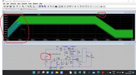
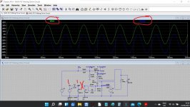
I've just tweaked the simulation to add a switch on surge to the audio input voltage. The input voltage now has a sudden DC shift as power is applied. That must happen in reality.
The FET's can not mute until there is enough negative voltage on the gates to turn them off.
The sim shows a brief pulse or thump getting through at switch on. The green trace is the signal from the preamp, the blue is the output from the mute circuit.
Attachments
you do get a very minor thump on start up
if the idle current on an amp is 26-30mv, is it critical if it was say 24 or 25mv?
if the idle current on an amp is 26-30mv, is it critical if it was say 24 or 25mv?
Not critical at all. Anything over a couple of milliamps idle current will effectively remove any audible distortion (crossover distortion).
With an amp like the NAD it is best to err on the side of safety and not set the bias current to high where it might run the risk of thermal runaway due to poor bias control.
With an amp like the NAD it is best to err on the side of safety and not set the bias current to high where it might run the risk of thermal runaway due to poor bias control.
so im just starting to understand some of this stuff
so if i look at this right,there will be a slight delay while the caps charge before there is enough voltage to turn on the fets?
so if i look at this right,there will be a slight delay while the caps charge before there is enough voltage to turn on the fets?
The FET's behave a little differently to how you might expect. You are used to ordinary transistors where you have to make a point of turning them on to get them to conduct.
When there is no gate voltage present (or more correctly when the gate/source voltage is around zero) then the FET is actually already on. It already conducts from D to S without you needing to apply voltage.
That means the NAD is unmuted in that condition and that is exactly what happens at the instant of switch on.
To turn the FET off and so make it 'open circuit' so it doesn't pass the audio means we have to take the gate negative with respect to the source and that takes a little time as the caps charge and that negative bias supply is established.
The FET also turn off more and more as the negative voltage increases. So at -1 volt its more on than off, at -2v its starts to turn off a bit more and so on. When we reach about -6 volts it is getting to be more properly off.
So in the time it takes for the gate voltage to reach around -6 volts the FET is passing all the things we are trying to block. It is a very imperfect solution to the problem but it is cheap and easy to implement.
What the NAD really needs is a proper speaker relay or solid state switch to only connect the speakers after a few seconds have passed and to disconnect the speakers pretty instantly power is removed.
oh i see well my thinking was right, if a bit reversed 😀
so you could modify this with a timed relay then
so you could modify this with a timed relay then
Easy to add as a little diy project I would say.
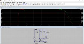
Try these. The first one gets its supply from the main DC rail in the amp. The disadvantage of this is that the relay does not drop out instantly at switch off but holds on as the rail falls. In many amps that would not be a problem because the amp keeps working for a while as the rails fall. As long as the relay drops out before the amp makes any noises then its not a problem.
The second one generates its own rail from the AC of the transformer. The reservoir cap is scaled to allow a fast drop out.
The trace shows the relay current and its timing relative to the applied supply voltage.
(The FET's used in these are power FET's and these type are normally off and only conduct when a G-S voltage of about 4v and higher exists)
Attachments
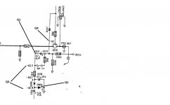
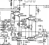
just a few questions about the attached
Afterlooking at your sim it makes more sense to me how the FET works with the
they are or will be obvious to you guys but i need to ask so i can understand if im looking at this correctly
Q1-i presume when the switch is closed the cap cannot charge
cap 531 is in parellel with R519?
Q2-why do you have a diode here?if it wasnt there what difference would it make?
Q3-why do would you start off with -30v, go up to -60v then back down to -20v
why not just go to -20v
Q4-how does this voltage suddenly become 0.5v
in your sim,if you also remove the diode D3 it appears to have no real impact,does this need to be there, like in the diagram?
🙂
Attachments
Imagine the circuit without the switch contact or R519. The circuit works normally at switch on.
When you switch off two things happen:
1/ The switch immediately shorts out the cap and so that instantly applies a negative voltage to the FET gates and so mutes the signal. That negative voltage is the -62 volts on the diagram.
2/ By shorting the cap out it removes charge on the cap and so the circuit is ready to start again should you suddenly switch on.
R519 limits the discharge current of the cap into the switch contacts. Even a little cap will pit the contacts if repeatedly shorted out by the contacts.
The voltage from the transformer is lets say a 30 volt peak voltage, that's 60 volts peak to peak or about 21 volts AC if read on a meter.
The peak voltage goes 30 volts above ground and 30 volts below ground.
Capacitor C532 AC couples that voltage and so removes its absolute reference to ground. Remember caps do not pass DC.
So the output of the cap is now of the same amplitude but 'floating'. Its reference point to ground has gone.
D506 is used to 'clamp' the voltage and tie it to ground. The AC voltage (the 50Hz sine wave) is now clamped to ground and swings 60 volt below ground. The diode conducts when the voltage tried to go above ground and so the net effect is that the whole waveform shifts level downwards.
So we have level shifted the AC voltage from -/+30 volts that was ground referenced to one that is now 0 to -60 volts ground referenced (referenced via the diode).
D505 is a simple half wave rectifier used to generate a stable -60 volt rail from the 60 volt sine.
Look at the sim here. There is just the cap and diode in circuit. See how it level shifts the AC voltage. If we reverse the diode we would shift the waveform 60 volts positive.
Attachments
cheers for that, i will work my way through what you have said, as i understand some but not all
OK 🙂
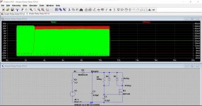
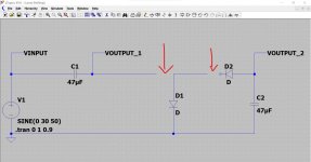
Try this and look at the waveforms of the labelled sections. After you have run it add the two missing links and then running the sim again before adding the next one.
Without the links you will see VINPUT and VINPUT_1 are the same but the VINPUT_1 end has no knowledge of ground. It is floating.
With the first link added the voltage is now clamped to ground via the diode D1.
The second link adds a rectifier to give us a smooth negative DC voltage from the level shifted sine.
If the level shifting was not done then we could only ever get a negative 30 volt rail from the input voltage. Doing it this way gets us the full 60 volt.
It is a simple Voltage Doubler.
Attachments
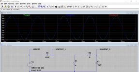

is there a reason why the waveforms are different on V1 output to V2 output?
so i do now see what you mean.
i guess this is what it would look like on anoscilloscope?
i dont have one of those, as im not sure i would realy benifit from having one yet.
so i do now see what you mean.
i guess this is what it would look like on anoscilloscope?
i dont have one of those, as im not sure i would realy benifit from having one yet.
In the first waveform diagram VINPUT and VOUTPUT_1 are overlaid on each other. They are the same.
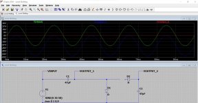
In the second waveform diagram we shift the level so that the AC sine voltage goes from 0 to -60 volts instead of going from +30 and -30 above and below ground.
In the third image we rectify that -60 volt peak to generate a smoot 60 volts DC.
(A scope is the single most useful bit of kit you can have imo. It tells you so much about what is happening in a circuit)
oh i see well my thinking was right, if a bit reversed 😀
so you could modify this with a timed relay then
so it is definatly the idle current i think is casing the distortion.
i have no current at all across RX1 or RX2 with temp trimmers fitted across R653 and R654, no current at all, so this is the starting point
Slow down 🙂
The relay is to prevent switch on and switch off noise, nothing else.
The voltage across R653 and 654 is used to determine idle current. The voltage across RX1 and RX2 does not tell us anything about the idle current.
Reducing the value of RX1 will turn OFF Q609 which allows the idle current to rise. It is very easy to cause damage by reducing RX1 to much.
If you really have no idle current at all then check the voltage across Q609 C to E. You will not see any idle current until you have at least 2.5 (ish) across the transistor.
Attachments
- Home
- Amplifiers
- Solid State
- NAD 3020b