wow interesting discussions, I've not even started yet lol 👍
I take from the market place, more often than not amps that people are prepared to dump or throw away, and i bring them back from that to be enjoyed by others for a few more years hopefully.
hopefully people can see what i have done so far at least improves the aesthetics of such a model(for those who like that sort of thing) 🙂
Im certainly not going to butcher it, i don't butcher anything, and it will be left so that the old transistors could be re installed at some point if required, for me presently its about possible improvements, interesting upgrades etcStill not convinced that a NAD3020 in 'almost mint condition' deserves such a butchering.
I take from the market place, more often than not amps that people are prepared to dump or throw away, and i bring them back from that to be enjoyed by others for a few more years hopefully.
hopefully people can see what i have done so far at least improves the aesthetics of such a model(for those who like that sort of thing) 🙂
In reference to #20 -
Good question and one I wasn't aware of before blowing several epi types myself, many years ago. Usually, the hometaxial types were RCA product, as originally specified but when they became EOL, I believe Motorola/onsemi still produced 2N3055H which have been said here as being hometaxial. However, I think member wg_ski has much more experience with picking these early types as they become available on the 'net and at auctions.
Personally, I've found several unexpected brands, even Toshiba branded 2N3O55's fitted as original semis in mostly 3020E and 7020E versions so it seems Proton were ordering the power transistors for later models wherever they could find a willing fab.
Motorola never did make a hometaxial anything - the process was RCA proprietary. Many others had similar “single diffused” processes. The ones from Solitron, BEL, even Toshiba fall into that category. RCA or rather the conglomerate it became with GE and Harris, made both in the 1980-85 years, so the H was used to designate which. Eventually it was dropped, and most of the time you got epitaxial. Many of those found their way into the NAD product. Motorola made the “HV” or “A” version, which was just a 100+ volt version, but was still a variant of epitaxial (closer to their 2N3773). Now you just get the MJ15015, but IMO they are not as good. They tend to sit at the low end of the gain spread because the guaranteed breakdown voltage is up at 120 and the two are inversely related for a given process.
The way to distinguish between the two is the much higher capacitances and higher base-spreading resistance of the homo types. Both are fT killers, and especially together.
The way to distinguish between the two is the much higher capacitances and higher base-spreading resistance of the homo types. Both are fT killers, and especially together.

so i have all the bits i need to start doing this
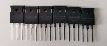
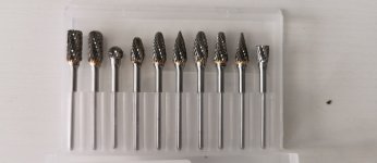
the FETS arrived today as did the sheet aluminium that i was going to use to make the new heatsink and milling bits that i will need to make the new openings but..........
i found a few old bits of IT kit in the bin so i nabbed the old heatsink off it, so i may look at using that.
not cheap this development bit, but its great fun
Attachments
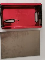
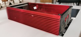
Nope its out of an old server array at workThat looks like a car amplifier chassis. Red heat sinks to give it the bling factor.
I don’t usually run into that many Philips transistors other than small signal TO-92s in my surplus travels. Gotta be careful when you run into those because the pin out is backwards. “Philips ECG“ doesnt count since they just come from the OEM get re-packaged and marked way up. Even the original Philips BD139/40 are rare birds these days.have you ever been interested in the Philips BD183?
BD181/2/3 is listed in a 1982 RCA/Harris data book I still use - they look like voltage-graded 3055H’s.
the FETS arrived today
Lateral FET's are a thing of beauty it has to be said 😉 and a red heatsink as well 👍
I think it will be ideal. It has a thin base so heat transfer will be quick to the main sinkLateral FET's are a thing of beauty it has to be said 😉 and a red heatsink as well 👍
Is see what you mean. Use heatsink compound where you have metal to metal contact as that will greatly improve heat transfer.
so i will be starting on this heatsink later today.
It is going to need some carefull thought about how they are going to be possitioned because of the resistors, but im sure i will work it out
its likely to be on the print side
It is going to need some carefull thought about how they are going to be possitioned because of the resistors, but im sure i will work it out
its likely to be on the print side
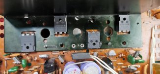
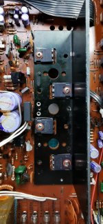
OK so alot of work for nothing realy today with that heatsink. It's too big, so I'm using one from a mk1 version, you can tell its an early one as it doesn't have the double fold. But the FETS are in, and now I've just got to work out the rest, just dry fit for now and I've had to put micas on the back as they are not all plastic, but metal backed
Attachments
Last edited:
so the plan is now, that i want to do as little damage as possible, so that it can at any time be converted back
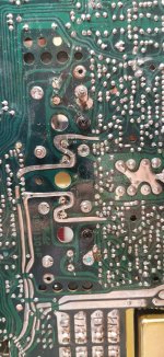
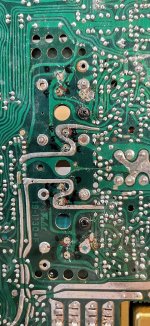
so the base/gate connection -i will make 2 cuts one near the main transistor connector and one further back.Then i can solder the resistor to the leg and to the print a little way back, i will also heat shrink these so they can short on anything.These can then be easily re joined at a later date if required.
Now the drain and source connections have to be swapped over, but there is a problem here, i cant cut the print or it will disrupt the on going connections so my thought is to slightly enlarge the hole of the current collector and sleeve/heatshrink the leg, then bend it over so it is close to the board, it can then be soldered to the emmiter connection(source) with a short hard wore connection, and i will do the same with the emmiter and connect it to the collector(drain)
it can be done neatly without destroying it that way
Attachments
Its all looking very neat. What I would say is check, check and check again before finally soldering. Look at each transistor in turn, make sure you have the N and P channel parts in the right places and that each lead of each one goes where it should.
The Drain goes where the collector would have been and the Source to where the emitter was.
Also you should at some point (temporarily) remove the two fixed bias setting resistors. Hopefully when all is OK we can use a preset (and if you like drilling holes in boards 😉 then you could maybe think of fitting a permanent preset) but if not we need a way to select and fit new value fixed resistors.
Oh I can fit them OK, those 2 on the board though are proper tight next to each other so it won't be easy with presets. One might have to go on the print sideIts all looking very neat. What I would say is check, check and check again before finally soldering. Look at each transistor in turn, make sure you have the N and P channel parts in the right places and that each lead of each one goes where it should.
The Drain goes where the collector would have been and the Source to where the emitter was.
Also you should at some point (temporarily) remove the two fixed bias setting resistors. Hopefully when all is OK we can use a preset (and if you like drilling holes in boards 😉 then you could maybe think of fitting a permanent preset) but if not we need a way to select and fit new value fixed resistors.
View attachment 1078706
Its only one preset per channel, one preset to replace both resistors... maybe I'm not following you there. Fitting on the print side is fine as long as you can get at them.
Sounds like a plan. So its either fit a preset as a permanent fixture or rig a preset temporarily with a view to adjusting it and then removing and fitting two new fixed resistors back in its place.
Up to you which...
Up to you which...
- Home
- Amplifiers
- Solid State
- NAD 3020 Series 20 mk-3 MOSFET Output Conversion