I have a problem with electrolytics in the input path -- the charge takes time to dissipate thus biasing the JFET gate. Even when you short the sending node you'll see the charge build back up. They are also a source of noise.
The optocoupler which Scott specified was in very short supply during the lockdowns, now available.
The optocoupler which Scott specified was in very short supply during the lockdowns, now available.
I intend to build it, of course.Have you built ?
Can you show some measurements ?
Patrick
As I understand, the optocoupler forms a control loop for the bias in the original circuit. Does it also stabilize the bias versus temperature?
Drift with temperature is not modelled in any of the spice models for jfets that I have.
Yes, I'm aware of the problems. For example, leakage is a significant noise source in electrolytics. For measurement amp duty, jfet input is a must, as is film cap coupling.I have a problem with electrolytics in the input path -- the charge takes time to dissipate thus biasing the JFET gate. Even when you short the sending node you'll see the charge build back up. They are also a source of noise.
The optocoupler which Scott specified was in very short supply during the lockdowns, now available.
Thanks for the info on the gate driver. The original circuit is very good, I'm sure. I do not wish to pollute the thread, just to share the idea (a starting point really), others might have difficulty sourcing that part.
Last edited:
The optocoupler allows you the luxury of going beyond the supply rails...when I first built the unit I used a larger cap on the opto biasing circuit -- bad idea -- it takes a long time to charge!
There is a biasing "optimum" for the JFET which neutralizes temperature drift. the graph was on Erno Borbely's JFET paper in AudioXpress, https://audioxpress.com/article/JFETs-The-New-Frontier-Part-1 figure 3B. Looks like 12mA for the SK170.
There is a biasing "optimum" for the JFET which neutralizes temperature drift. the graph was on Erno Borbely's JFET paper in AudioXpress, https://audioxpress.com/article/JFETs-The-New-Frontier-Part-1 figure 3B. Looks like 12mA for the SK170.
Yes, I know about the zero tempco bias point. I always check the Id curves in the datasheets for Vp+0.6. For many low noise jfets it is impractical to bias at the zero tempco...
I had this horror with the negative Input impedance with virtually all
feedback amplifiers of the form CS - Cascode - OpAmp - feedback to source, even
designs of the gods, like Horowitz&Hill etc. Propagation through the OpAmp
is simply to slow (costs phase margin). Add an inductive signal source and you've
got an oscillator. In Spice, you can simply plot V(signal generator) / I (signal generator),
TI 3.5 GHz CFBs after the cascode seemed to
work, but they drowned the signal in 1/f noise, even after 30+ dB of preamplification.
I then decided to go without feedback. To get somewhat stable gain, I temp-stabilized
the FETs at +40°C with a regulated oven. That was no real advantage.
FETs have both a positive and a negative TK, and they cancel at a certain drain
current. In simulation at 45 mA for 16 CPH3910. gm of the FETs changes with sqrt(Id)
so the aberrations are not too severe.
Avoiding feedback felt like a personal defeat, so I recently did a redesign with emitter
follower & RF transistors. boards are somewhere between JLCPCB/China & here.
It took 2 sot-89 transistors because of power dissipation.
I had a bias regulation loop patterned after the 70pV/rtHz amplifier from AOE3,
but at sub-Hz you cannot really say if it is noise or servo oscillations. Measuring
it takes eons. Yes, I'm more into measurements than Golden Ear audio.
Funny values like 0.1pF are the remains of what/if checks.
Ideas welcome.
Gerhard
Attachments
Last edited:
I believe that the reason shorting the sending node doesn't really work is that the electrolytic capacitor has some electrochemical process which needs a lot of time to stabilize.I have a problem with electrolytics in the input path -- the charge takes time to dissipate thus biasing the JFET gate. Even when you short the sending node you'll see the charge build back up. They are also a source of noise.
One can servo the amplifier (see Marco Rep's review of the Euler LFLNA
Fascinating stuff, probably worth a master's degree student writing a thesis.
I also made some experiments feeding the sources from a
current mirror CCS for DC and shorting the sources ac-wise
to GND with a large electrolytic. Allowed the gates to be at
0V. A giant failure if there ever was one.
I took an Oscon and got a 1/f corner of several KHz++
and levels that sent the FFT analyzer to overflow.
Nippon Chem. Alu was much better but still unusable.
An AVX wet slug tantalum 4700u/25V for $100 was borderline
ok, but not really.
BTW Vishay wanted twice that $$$.
It seems with that architecture you see every electron that
escapes through the source capacitor, with 0.6V across it
and 25V rated.
Thinking about it, the CCS source impedance was needlessly high.
Last edited:
According to the author, this one worked well. The input is not a feedback amp, so shouldn't have problems with negative input impedance. First stage is common source IF9030, source resistor is shunted by 180mF (yes millifarads). He used Nichicon VK electrolytics for this.
https://web.archive.org/web/20170829110836id_/https://users.cosylab.com/~msekoranja/tmp/04447683.pdf
https://web.archive.org/web/20170829110836id_/https://users.cosylab.com/~msekoranja/tmp/04447683.pdf
I have actually built the Levinson using 2SK369 years ago.
0.1Hz to 10Hz is not really important for my purpose.
Patrick
0.1Hz to 10Hz is not really important for my purpose.
Patrick
Why not servo the drain current , use all dc coupling, and regulate to the drain current at zero vgs (idss).
electrochemical currents are very very noisy, and have always a 1/f behaviour, so we need to avoid them at all cost.
electrochemical currents are very very noisy, and have always a 1/f behaviour, so we need to avoid them at all cost.
Hi @EUVL
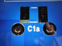
Thank you for making the gerbers available. I've had both N and P channel boards made and noticed that C1a is shorted on the ground trace on the PJFET board, rather than connecting across C1 as you did with the N channel board. Also noticed that the R2a label is missing. Just mentioning these in case you hadn't noticed before.
Thanks again.

Last edited:
Was ages ago. I forgot what I did then.
Good that you are checking everything first.
Let us know how you get on.
Patrick
Good that you are checking everything first.
Let us know how you get on.
Patrick
The box is ordinary microwave stuff; it would be costly only if milled
just for the dimensions I want. But I can cut the vector board for the
boxes that I have. The circuit on the vector board is not exactly a
work of art. Just good GND distribution on the top side.
A good source for the milled boxes are wideband microwave
electronis from ALI. Just remove the innards.
If you insist in new boxes, see for example
< https://telemeter.info/de/mwdownloads/download/link/id/786 >
There should be similar sources around the world.
Gerhard
As the En of the source resistor become less than 0.7071 * En of the JFET, its overall noise contribution becomes less relevant, is that not so?According to the author, this one worked well. The input is not a feedback amp, so shouldn't have problems with negative input impedance. First stage is common source IF9030, source resistor is shunted by 180mF (yes millifarads). He used Nichicon VK electrolytics for this.
- Home
- Design & Build
- Equipment & Tools
- My version of the G = 1000 low noise measurement amp (for Ikoflexer)
