The link is correct though. Anyway, I'm sure you simulated the correct one. This one, from post 407.
It is stable in reality. Built a few, and not just me.
An externally hosted image should be here but it was not working when we last tested it.
It is stable in reality. Built a few, and not just me.
Hi,
If the circuit on page one of this thread is the correct up to date one, it would not simulate stable for me.
WTF, somebody please post the final schematic in this thread. There are to many schematics floating around, all linked to websites, apparently shapeshifting as we speak. It starts to remind me of the Krill threads 🙂
I still have the test bed, I can redo some measurements if the schematic is different. I may also have some suggestions for improvement, things like frequency compensation and decoupling 🙂
BTW, for simulation, this thing requires the Middlebrook theorem and method. The feedback network is significantly loading the base amp.
Last edited:
I get exactly the same result with Middlebrook's method as I get with Tian's method. For those of you with ltspice, you can check this easily. The Middlebrook method and the Tian method are both implemented in files included with ltspice: LoopGain.asc and LoopGain2.asc, respectively.
Could someone please post the circuit image from my previous post? I don't think syn08 can see it because I'm on his ignore list. Talk about someone shooting himself in the foot and the making a big fuss about the guy that put the foot there. 🙂
Could someone please post the circuit image from my previous post? I don't think syn08 can see it because I'm on his ignore list. Talk about someone shooting himself in the foot and the making a big fuss about the guy that put the foot there. 🙂
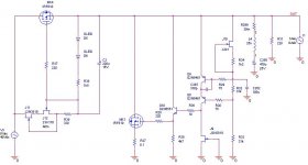
Latest schematic:
An externally hosted image should be here but it was not working when we last tested it.
This compensated version should have decent performance. It's by no means optimized, but the phase margin is over 80 degs and the unity loop gain frequency is 1-2MHz. Overall performance is a compromise, of course, between loop gain and stability.
The output cap parasitics are typical for a good quality electrolytic. It largely impacts the stability, more than I would like, but it should work as it is.
Optimization may include a lead-lag compensation of the gain stage (instead the brutal Miller of C267), somebody may pick up from here.
Noise simulation is here nonsense. None of the active devices have realistic noise models (if at all). In my libraries, 2N5551 has Rbb'=10ohm, in real life is 40-60ohm (and the noise gets amplified by the error amp, so the output noise is significantly impacted).
I've already spent enough time on this topic and thread, I'll leave for now. Take care with those PCB prices for the GB! The same www.barebonespcb.com will do 100 2" x 3" boards for $3.50 a pop plus shipping. Without solder mask and legend and on regular 1.6mm vero substrate, but that's all what this toy deserves and is worth of. All active parts except 2SK170 (which is not really required, overall noise is not that good anyway) are available through DigiKey and Farnell.
Bye.
Attachments
Salas, do you remember all those many pages of discussions we had (which some don't read) and how we addressed compensation with small capacitors and all kind of other tricks?
Because there are so many pages in the thread, not to even mention the simplistic thread, people might not realize how much we've discussed these issues before. Then someone comes and says the result is "crap" (he did say that in the message above), he makes all kind of mistakes, throws in a capacitor and says that he saved us from ourselves. It's pretty sad, really.
syn08, you might get better simulation results if you turn those LEDs around. While you're at it, turn C3 around too.
Me I will just put one of yours together when you send me boards and some difficult semis for me to get locally, apply it on a 61dB phono, I have one reg of mine in it, and will run an FFT for total noise floor on the output with input shorted. With both regs. If there is no problem with extra noise rising up, I will listen to records. I will let you know. I am not EE so I can't be sure of anything deep electronics analysis. We just try to be a bit creative and the proof is in the pudding as they say. Even if its no good its still yours and makes you learn, and we all learn together. If it gets some debugging we will try this and that and have fun. That is all in a hobby IMHO. At least you can run some sims for ideas, because me I am only practical, can't make out where the lib directories go yet!😀
Don't worry Iko, I trust you, so I buy your pcbs. About test I am sorry mine friend is very busy & can't do it in a very reasonable time so can't count in him.
merlin, thank you. It's ok, we might yet find someone else who can run measurements. I'm not in a hurry.
@salas We are in agreement on this one, it's a hobby, I intend to keep it enjoyable. 🙂 Regardless of the GB, as we have talked in the past, I will send you pcbs (and those pesky semis) because I will have some made anyway. Hey, I'm not an EE either.
I've found the noise measurements, see attached.
510nV/rtHz plateau noise, up to 11,000nV/rtHz at very low frequencies (1Hz). Corner frequency is around 100Hz, not bad.
This is in my book "noisy as hell". Imagine you would try to feed a MC stage with this regulator. To keep the power supply negligible, the MC stage would need a HF PSRR of not less than 60dB. There's not many low noise opamps with such a PSRR, for a full discrete low noise design that's almost impossible to get.
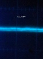
I would like to address this now. In the past I have posted pictures taken of my oscilloscope screen while the regulator was connected. The oscilloscope was set on the most sensitive setting, i.e. 100uV/div. What this means is that if there was ripple with peaks spanning from one horizontal line to the next horizontal line shown on the oscilloscope screen, it is equivalent to measuring 100uV peak-to-peak.
Attached is an image showing a close up of the trace, while the positive regulator is powered on. In the past I have assessed the trace width to between 30 and 40 microvolts, because I wanted to err on the plus side. It is definitely below 50 microvolts, which would be 1/2 of division.
Now, let's see what syn08 has measured. He reported a noise density of 510nV/rtHz. We need to convert this to a peak-to-peak value, such as what I have shown in the picture. It is typical to take a frequency range of 21kHz for the conversion, since we want to know the peak-to-peak value especially in the audio range.
The proper way to convert is to integrate below the curve that syn08 has shown. However, a good approximation can be give by the following formula:
Peak-to-peak noise = ND * sqrt(frequency) * 1.57 / 0.707
We assume a 1 pole filter to discard the rest of the frequency above 21kHz, hence the multiplication by 1.57, and we divide by 0.707 to convert from RMS to peak-to-peak. So,
syn08_p2p_noise = 510 * sqrt(21000) * 1.57 / 0.707
syn08_p2p_noise = 164119.45347 nV = 164uV
A little tutorial on converting spectral density to RMS can be found at this link from AD:
Analog
164uV would have shown as a very thick trace on my oscilloscope, spanning across almost two horizontal lines on the screen.
Attachments
does divide by 0.707 give Vrms to Vpk or gives Vrms to Vpp?
Your noise on the scope looks like 20 to 30uVpp as best as I can interpret. But it appears to be wideband, not filtered @ an audio frequency.
If you increase the noise bandwidth then the predicted 164uV will be even higher for the actual scope picture.
Ther is obviously something very different between the actual noise measurement and the noise prediction.
Iko, it's not necessary for me to test the pcbs, please send me mine pcbs with all semis package & tell me by pm the total cost of them, if possible I want to pay by Paypal, thks.
does divide by 0.707 give Vrms to Vpk or gives Vrms to Vpp?
Oops, you're right, it's voltage peak. This should teach me to not write things when half asleep. 🙂
Multiply by 2 and you get Vpp. And this makes things even worse for syn08's result, of course, because what's shown on my scope is Vpp. Thanks for the correction Andrew!
Your noise on the scope looks like 20 to 30uVpp as best as I can interpret. But it appears to be wideband, not filtered @ an audio frequency.
If you increase the noise bandwidth then the predicted 164uV will be even higher for the actual scope picture.
Yes, you're right. I just wanted to approximate in such way that it would be a bit of advantage for his argument, and even so, it still shows much smaller noise for my measurement.
Ther is obviously something very different between the actual noise measurement and the noise prediction.
Andrew, he didn't say it was a prediction, he said he measured it. The fact that there is a big difference is my point, and he must have made a mistake either measuring or building the regulator. The schematic he shows does not work and has one big error: The LEDs that bias the CCS mosfet are reversed, and so is the capacitor. I wonder if his simulations and circuit have the same error.
@merlin, ok with me. Please be a only a bit patient until I clear this mess up.
Would´t it be a good idea to integrate the mountings for a SK104 heatsink?
For those who want to place the pcb not at a side of a enclose, this makes it much much easier. 😉
Sorry I missed this question in the heat of the many messages here.
For small currents that would be ok, and the heat sink can be attached to the mosfet as is. The problem with adding mounting on the pcb for the SK104 would be that I'd have to make the board extend a bit more at the back of the mosfet, and then those who want to run larger current can't attach to the side of case of larger heat sinks. See what I mean?
But a similar size heat sink to sk104 isn't too large so it can be mounted on the mosfet without being attached necessarily to the board. So we're not missing anything, I think.
I would like to address this now. In the past I have posted pictures taken of my oscilloscope screen while the regulator was connected. The oscilloscope was set on the most sensitive setting, i.e. 100uV/div. What this means is that if there was ripple with peaks spanning from one horizontal line to the next horizontal line shown on the oscilloscope screen, it is equivalent to measuring 100uV peak-to-peak.
Attached is an image showing a close up of the trace, while the positive regulator is powered on. In the past I have assessed the trace width to between 30 and 40 microvolts, because I wanted to err on the plus side. It is definitely below 50 microvolts, which would be 1/2 of division.
Now, let's see what syn08 has measured. He reported a noise density of 510nV/rtHz. We need to convert this to a peak-to-peak value, such as what I have shown in the picture. It is typical to take a frequency range of 21kHz for the conversion, since we want to know the peak-to-peak value especially in the audio range.
The proper way to convert is to integrate below the curve that syn08 has shown. However, a good approximation can be give by the following formula:
Peak-to-peak noise = ND * sqrt(frequency) * 1.57 / 0.707
We assume a 1 pole filter to discard the rest of the frequency above 21kHz, hence the multiplication by 1.57, and we divide by 0.707 to convert from RMS to peak-to-peak. So,
syn08_p2p_noise = 510 * sqrt(21000) * 1.57 / 0.707
syn08_p2p_noise = 164119.45347 nV = 164uV
A little tutorial on converting spectral density to RMS can be found at this link from AD:
Analog
164uV would have shown as a very thick trace on my oscilloscope, spanning across almost two horizontal lines on the screen.
Iko,
You are on the right track but a few things need to be clarified.
a) How and where is the 21kHz LPF implemented. If you have the cro probe
directly on the reg OP then there is no LPF except for the Cro/probe BW
itself. The cro does not 'hear' the noise, it sees everything there within it's
BW limitations.
b) When you attach the cro probe to the reg OP, discard the earth lead and
push on clip. Attach the shortest possible lead from reg ground point directly
to the cro probes earth 'ring' whilst holding the tip onto Reg OP. A lot of the
apparent noise can actually be the earth lead picking up noise / RF.
c) You have a 1.41 P-P -> RMS conversion factor. For Gaussian noise it
is closer to 6. So RMS = P-P on cro / 6.
So for a wide band rough stab at noise measurement off screen, a BW of
1MHz can easily be used. As such, nV/rtHz from pk-pk on screen can be as
low as p-p / (1000 x 6). It all depends on the noise source and measurement
BW.
As you can see there are a lot of variables and it really only serves as a
very rough guide. Best way to do it is make up simple x 1000 amplifier
using AD797 etc and implement LPF at OP. Then you can measure much
more accurately.
Having said all of the above, this design should be able to acheive very low
noise, easily below 20 nV/rt Hz with good layoutand component selection.
cheers
Terry
Nice to hear from you again Terry. Your observations are always appreciated.
You probably didn't read all the sordid details and I don't blame you. Another member of this forum has implemented this design and reported terrible noise of about 510nV/rtHz. Whereas I had observed a peak-to-peak noise of perhaps 30uV, as you can see in the image I posted above. Then I wanted to convert his 510nV/rtHz to peak-to-peak so that we could compare our results. If my result were within 10% of his result then we could be pretty confident the two implementations are in sync. I suppose I could also have converted my peak-to-peak value to spectral density and compare with his result. In any case, I took the 510 nV/rtHz plateau result and converted it to p-p. I chose 21kHz arbitrarily, in part because it's a frequency range often chosen when dealing with audio devices; had I chosen a wider bandwidth syn08's result would look even worse.
Yes, good point, thank you! I have also read Bob Pease's little article about this not very long ago.
What's All This Ground Noise Stuff, Anyhow?
However, I confess I didn't do it to capture the trace I showed earlier. Even so, the observed noise was quite small and seeing that I simply didn't obsess any more over it.
Interesting, I didn't even think about the noise distribution. If we assume it Gaussian and apply your formula, we get even worse a difference between syn08's result and mine.
Let's see.
syn08_p2p_gaussian_noise = 510 * sqrt(21000) * 1.57 * 6 * 2
syn08_p2p_gaussian_noise = 1.39mV
We'd get a larger number using a wider bandwidth, but there's no point in continuing this. I think it's pretty clear that my implementation and syn08's implementation of the same circuit are completely different. I don't blame him for being so outraged, his result is indeed a disaster.
You mean if I observed 30uV pk-pk on screen, that would convert to 30000 / (1000 * 6) = 5nV/rtHz ?
I plan to do this with the AD797 as you suggest because my current "noise" amp is using 2sk170s in three stages and something based on the AD797 would most likely be better.
I put quite a bit of effort in the layout design. This is it:
I realize you have your life and are busy and I'm definitely not asking you to check the layout. I'm just saying. The features I tried to optimize were low output impedance and low noise. Tried my best to make short, straight, and wide power tracks, to minimize inductance, enough distance between tracks to minimize capacitance, ground "island" so no ground loops.
Iko,
You are on the right track but a few things need to be clarified.
a) How and where is the 21kHz LPF implemented. If you have the cro probe directly on the reg OP then there is no LPF except for the Cro/probe BW itself. The cro does not 'hear' the noise, it sees everything there within it's BW limitations.
You probably didn't read all the sordid details and I don't blame you. Another member of this forum has implemented this design and reported terrible noise of about 510nV/rtHz. Whereas I had observed a peak-to-peak noise of perhaps 30uV, as you can see in the image I posted above. Then I wanted to convert his 510nV/rtHz to peak-to-peak so that we could compare our results. If my result were within 10% of his result then we could be pretty confident the two implementations are in sync. I suppose I could also have converted my peak-to-peak value to spectral density and compare with his result. In any case, I took the 510 nV/rtHz plateau result and converted it to p-p. I chose 21kHz arbitrarily, in part because it's a frequency range often chosen when dealing with audio devices; had I chosen a wider bandwidth syn08's result would look even worse.
b) When you attach the cro probe to the reg OP, discard the earth lead and push on clip. Attach the shortest possible lead from reg ground point directly to the cro probes earth 'ring' whilst holding the tip onto Reg OP. A lot of the apparent noise can actually be the earth lead picking up noise / RF.
Yes, good point, thank you! I have also read Bob Pease's little article about this not very long ago.
An externally hosted image should be here but it was not working when we last tested it.
An externally hosted image should be here but it was not working when we last tested it.
What's All This Ground Noise Stuff, Anyhow?
However, I confess I didn't do it to capture the trace I showed earlier. Even so, the observed noise was quite small and seeing that I simply didn't obsess any more over it.
c) You have a 1.41 P-P -> RMS conversion factor. For Gaussian noise it
is closer to 6. So RMS = P-P on cro / 6.
Interesting, I didn't even think about the noise distribution. If we assume it Gaussian and apply your formula, we get even worse a difference between syn08's result and mine.
Let's see.
syn08_p2p_gaussian_noise = 510 * sqrt(21000) * 1.57 * 6 * 2
syn08_p2p_gaussian_noise = 1.39mV
We'd get a larger number using a wider bandwidth, but there's no point in continuing this. I think it's pretty clear that my implementation and syn08's implementation of the same circuit are completely different. I don't blame him for being so outraged, his result is indeed a disaster.
So for a wide band rough stab at noise measurement off screen, a BW of 1MHz can easily be used. As such, nV/rtHz from pk-pk on screen can be as low as p-p / (1000 x 6). It all depends on the noise source and measurement BW.
You mean if I observed 30uV pk-pk on screen, that would convert to 30000 / (1000 * 6) = 5nV/rtHz ?
As you can see there are a lot of variables and it really only serves as a very rough guide. Best way to do it is make up simple x 1000 amplifier using AD797 etc and implement LPF at OP. Then you can measure much
more accurately.
I plan to do this with the AD797 as you suggest because my current "noise" amp is using 2sk170s in three stages and something based on the AD797 would most likely be better.
Having said all of the above, this design should be able to acheive very low
noise, easily below 20 nV/rt Hz with good layout and component selection.
cheers
Terry
I put quite a bit of effort in the layout design. This is it:
An externally hosted image should be here but it was not working when we last tested it.
I realize you have your life and are busy and I'm definitely not asking you to check the layout. I'm just saying. The features I tried to optimize were low output impedance and low noise. Tried my best to make short, straight, and wide power tracks, to minimize inductance, enough distance between tracks to minimize capacitance, ground "island" so no ground loops.
- Status
- Not open for further replies.
- Home
- Amplifiers
- Power Supplies
- My take on a discrete shunt voltage regulator