Hi nelsonvandal,
Without trying a double or triple EF I can't say. But I do know from my testing that adding a CFP driver stage reduces the odd order harmonics by quite a bit. In Roender's simulations he found the CFP driver reduces 3rd, 5th, and 7th harmonics by about 20db. The cascode VAS has a similar effect on the even harmonics.
I think the listening test should be interesting.
I've attached a couple THD plots taken from my original boards with the same output devices, 50 volts rails, and 2n5551 inputs to compare with the new design.
Regards,
Al
Dear AAK,
Very nice plots. What is this "PHS" software you use? I tried googeling it but no results.
With kind regards,
Bas
http://www.diyaudio.com/forums/group-buys/156885-symasym-sequel-aaks-pcb-gb-19.html#post2301549........... where could I get the pcbs from?
Yes, i like to design PCB.
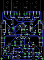
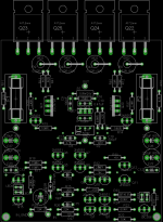
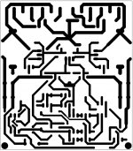
My PCB version of AAK's DTV rev_1.4 amp. May single layer PCB, friendly for DIYer.
Not Builded yet! may error, please double check if interest to used it.
PCB files on KICAD format.
Hi zharmo,
Can you post again your pcb layout, cant open in eagle software. I think its corrupted..Thanks for your reply..
Boyet
Hi, this is my first post in this forum. I am DIY entosiast, and i dont understand from schematics. I had build about ten amplifiers. All of them are from the internet and forums. I read the theme's of Roender for RMI-FC100 and i wanna make this amplifier, but it is expensive for me. Hard to find that expensive output transistors and match them. I like very much scheme's on AAK, and i have almost all the parts to do that. I made my own design of the board. The board is single side (easy to make by photo method). The dimension on the board is 80x90mm. It doesnt include the PSU. I place the psu on my designs close to amplifiers PCB, and with good ground wiring i dont have problem with hum or noise. I draw the schematic and design PCB for one day, thats why i need to check all for errors. If all is right i will continue with making the PCB.
I use Eagle 5.9. I will post pdf with shematic, and pictures on the PCB. If i make the amplifier and i am sure that the PCB is correct, and AAK allow me, i will load the PCB for making, who wont it. I apologise for my bad english.
Cheers, Christo!
I use Eagle 5.9. I will post pdf with shematic, and pictures on the PCB. If i make the amplifier and i am sure that the PCB is correct, and AAK allow me, i will load the PCB for making, who wont it. I apologise for my bad english.
Cheers, Christo!
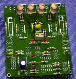
This is my version of the SYMASYM - the TO-3 version with CAP-multiplier:

http://www.abload.de/img/topviewgket.png
And it sounds very, very good.
Best regards - Rudi_Ratlos

http://www.abload.de/img/topviewgket.png
And it sounds very, very good.
Best regards - Rudi_Ratlos
This is my version of the SYMASYM - the TO-3 version with CAP-multiplier:
http://www.abload.de/img/topviewgket.png
And it sounds very, very good.
Best regards - Rudi_Ratlos
Rudi,
Like you already know I like it nice job
Feedback
Ithco,
In the schematic and on the board the feedback network is incorrect implemented.
Ithco,
In the schematic and on the board the feedback network is incorrect implemented.
Piersma thank you for see that. Can you explain me how to correct implement NFB, please? I would appreciate it.
Hi zharmo,
Can you post again your pcb layout, cant open in eagle software. I think its corrupted..Thanks for your reply..
Boyet
My PCB files is KICAD format, not eagle's pcb.
please open with KICAD, its free
@Itco,
this is how the NFB should look like:

http://www.abload.de/img/27.07p153.png
Best regards - Rudi_Ratlos
this is how the NFB should look like:

http://www.abload.de/img/27.07p153.png
Best regards - Rudi_Ratlos
incorrect implemented
Itco, also the input ground point is at the wrong end of the 10 ohm resistor and Q1 is reversed...
Regards,Loek
Itco, also the input ground point is at the wrong end of the 10 ohm resistor and Q1 is reversed...
Regards,Loek
No. Simply connect IN_GND to the lower end of C15 (SG).the input ground point is at the wrong end of the 10 ohm resistor
GND is correctly shown at the bottom of R39. In this schematic GND is actually PCB Power Ground (PG).
However, check the GND connection of the base of Q8 & R2+R3 & C17+C18 & R32.
It may be that performance could be improved if this GND were not on the PG.
Could it be moved to SG?
Can anyone enlighten me?
Where should Q8 base and all the other components on that net be connected?
Where should Q8 base and all the other components on that net be connected?
Hey Guys,
You're off topic. This is, My new SymAsym PCB design Rev_1.3 forum that also gets into my Rev_1.4 PCB design. The schematic posted by itco is from that design. Just thought I'd bring it up. Here's the builders thread for Rev_1.4 with schematics on Post #1 if you're interested.
http://www.diyaudio.com/forums/soli...-sequel-aaks-rev_1-4-pcb-builders-thread.html
Best regards,
Al
Hi AAK, thank you for the link.
Could u tell me please, is the value of VAS lead resistors is correct(i mean 47K)?
What is the model of the LED diodes?
Could u tell me please, is the value of VAS lead resistors is correct(i mean 47K)?
What is the model of the LED diodes?
...and AAK's design works mighty fine
Itco, look in here:
http://www.diyaudio.com/forums/atta...read-sts100_rev_1.4_assembly_instructions.pdf
Itco, look in here:
http://www.diyaudio.com/forums/atta...read-sts100_rev_1.4_assembly_instructions.pdf
Last edited:
- Status
- Not open for further replies.
- Home
- Amplifiers
- Solid State
- My new SymAsym PCB design Rev_1.3