@Elvee @Minek, Thanks for feedback.
I didn't do a quick dirty test during matching. With or without heatsink, first value and then stabilized value etc. Somehow devices have retained their gap in each condition then I assumed that method is fine. As you noted, actual circuit will decide.
I didn't do a quick dirty test during matching. With or without heatsink, first value and then stabilized value etc. Somehow devices have retained their gap in each condition then I assumed that method is fine. As you noted, actual circuit will decide.
Last edited:
Interesting real-world feedback: it is generally assumed that MOSfets of the same process can be matched accurately based only on a single pair of parameters.
It would be instructive to see what the dynamic behaviour is (I assume you measured the quiescent current).
Peufeu should have the means to test it in his measurement setup.
When he is finished with his main targets, he could investigate that particular aspect
I only tested 2 samples of IRFP240/9240, so caveat...
They had different Vgs tempcos (it also depends on Vds and current)
_Pulse_IRFP9240 Vishay.png")
_Pulse_IRFP9240 Vishay-1.png")
So if they have a bit different tempcos, and you measure them at ambient, they will no longer be matched when hot in the amp!
But they had exactly the same gm versus Id:


But... I used pulsed measurements: Vgs and Id are applied, then Vgs is measured a couple microseconds later.
Without the pulsed technique, looks like it's another can of worms...
It would not be difficult to do with a micro that has an ADC: just flip a MOSFET to connect a resistor from the source to a power supply to set current, and acquire Vgs with the ADC. An arduino can do that.
The subject seems worth investigating. I am probably going to explore it in the near future: that is something I can do with just my standard lab blocks, no need for a sophisticated test jig.
It is just necessary to build half of a PP, and drive it with a pseudo-class B signal whilst monitoring the current repartition between the matched (or not) devices.
It is simple, and should be reliable as it mimics the actual workings of a class B amplifier.
The tracking of the quiescent current might be desirable (I am not even sure about that*), but what counts for a PA is the correct sharing when it does heavy-lifting, at high currents, not during idle conditions.
*I suspect that uneven threshold characteristics might be beneficial, as it would spread the behaviour of the composite to look like a solid-state triode
Yeah, you could do pulsed measurements with a scope:
power supply -> drain
square wave -> gate
source -> resistor -> ground
Measure voltage on source resistor with scope. Easier with a digital scope which can measure the voltage at the top of the waveform and display it...
In fact if you average voltage with a RC filter, and use a low duty cycle square wave, you could even use a multimeter... Use a pulsed current source (ie, MOSFET, resistor, and square wave with 1% duty cycle), measure average of Vgs, multiply by 100 to compensate for 1% duty cycle, that would give Vgs @ Id,Vds without temperature drift...
Or use an analog sampler...
> *I suspect that uneven threshold characteristics might be beneficial, as it would spread the behaviour of the composite to look like a solid-state triode
Want me to test it?
If you feel like it, and have a sufficient number of slightly different devices of both sexes, yes, but before committing to hardware, it would probably be a good idea to test it in sim.Want me to test it?
It will spare a waste of time and efforts in case the results look unpromising.
A favorable sim is no guarantee of the validity in the real world, but the reverse is almost certainly true.
I'll setup a sim one one of these days
I have a bunch of IRFP240/9240.
I can use 2 pairs in parallel and shift the gates of one pair with diodes for example.
I can use 2 pairs in parallel and shift the gates of one pair with diodes for example.
There is a problem with the sim: with the IRFP240/9240 models, crossover artifacts are practically absent.
There is some droop in the Xover region if the bias current is really too low, but when it is high enough, only a hint of gm-doubling is barely visible.
Difficult to improve on that.
There is some droop in the Xover region if the bias current is really too low, but when it is high enough, only a hint of gm-doubling is barely visible.
Difficult to improve on that.
Attachments
There is a problem with the sim: with the IRFP240/9240 models, crossover artifacts are practically absent.
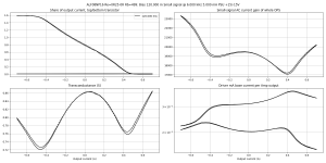
Your models agree with my measurements. These FETs produce a very nice crossover, but they need quite a bit of bias current to fill the gm hole in the middle. Plots below are one pair IRFP240/9240 with non-inductive 0R33 source resistors.
Can you post the same gm plot with your FQA models?
Attachments
-
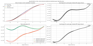 gm-Bias 400.000 m, PSU +20.0-20.0V,AC 64.000 mA 6.000 kHz,load 7.6R,HFin,LFout-IRFP9-240 v13 Re=.png204.6 KB · Views: 108
 -
 gm-Bias 300.000 m, PSU +20.0-20.0V,AC 64.000 mA 6.000 kHz,load 7.6R,HFin,LFout-IRFP9-240 v13 Re=.png195.3 KB · Views: 247
 -
 gm-Bias 200.000 m, PSU +20.0-20.0V,AC 64.000 mA 6.000 kHz,load 7.6R,HFin,LFout-IRFP9-240 v13 Re=.png193.6 KB · Views: 252
 -
 gm-Bias 100.000 m, PSU +20.0-20.0V,AC 64.000 mA 6.000 kHz,load 7.6R,HFin,LFout-IRFP9-240 v13 Re=.png175.4 KB · Views: 247
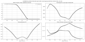
I measured FQP19N20/FQP12P20 a long time ago and they give a similar gm plot, very smooth.
But TO-247 versions FQA19N20/12P20 have been discontinued, leaving only TO-220s (FQP reference) which have high thermal resistance. And their tempco is much higher in the wrong direction than the IRFP's. Both factors combined mean the bias goes YOLO. Also, difficult to parallel, the hotter one will steal all the current. With the huge TO-247 package and very civilized tempco, IRFPs are super stable.
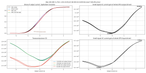
If your FET models give a gm curve that looks like that one below, a W shape with gm-doubling in the middle and two sharp corners at the bottom, then they're not modeling subthreshold correctly. Plot below is for ALFET lateral FETs.
But TO-247 versions FQA19N20/12P20 have been discontinued, leaving only TO-220s (FQP reference) which have high thermal resistance. And their tempco is much higher in the wrong direction than the IRFP's. Both factors combined mean the bias goes YOLO. Also, difficult to parallel, the hotter one will steal all the current. With the huge TO-247 package and very civilized tempco, IRFPs are super stable.
If your FET models give a gm curve that looks like that one below, a W shape with gm-doubling in the middle and two sharp corners at the bottom, then they're not modeling subthreshold correctly. Plot below is for ALFET lateral FETs.
Attachments
Last edited:
The good news is that, unusually, reality and models converge remarkably well.
The bad news is that these Fets are not good candidate to test the staggered Vto hypothesis in a // configuration.
I don't have models for the FQA's
The bad news is that these Fets are not good candidate to test the staggered Vto hypothesis in a // configuration.
I don't have models for the FQA's
The bad news is that these Fets are not good candidate to test the staggered Vto hypothesis in a // configuration.
Can you explain? I'm curious about why...
ThanksSee this file: http://www.minek.com/lib/minek.lib
The idea (maybe misguided) is to even out the individual quirks of each individual transfer function by having a sum of more or less random, slightly different ones (think of some kind of dithering, to refer to a contemporary concept).Can you explain? I'm curious about why...
If the transition region is already very smooth, there is probably little to be gained by smoothing it even more.
I've tried to do that in sim with BJTs but... unconvincing results, it moves the wiggles around on gm but doesn't get rid of them. No resistors is a lot better.
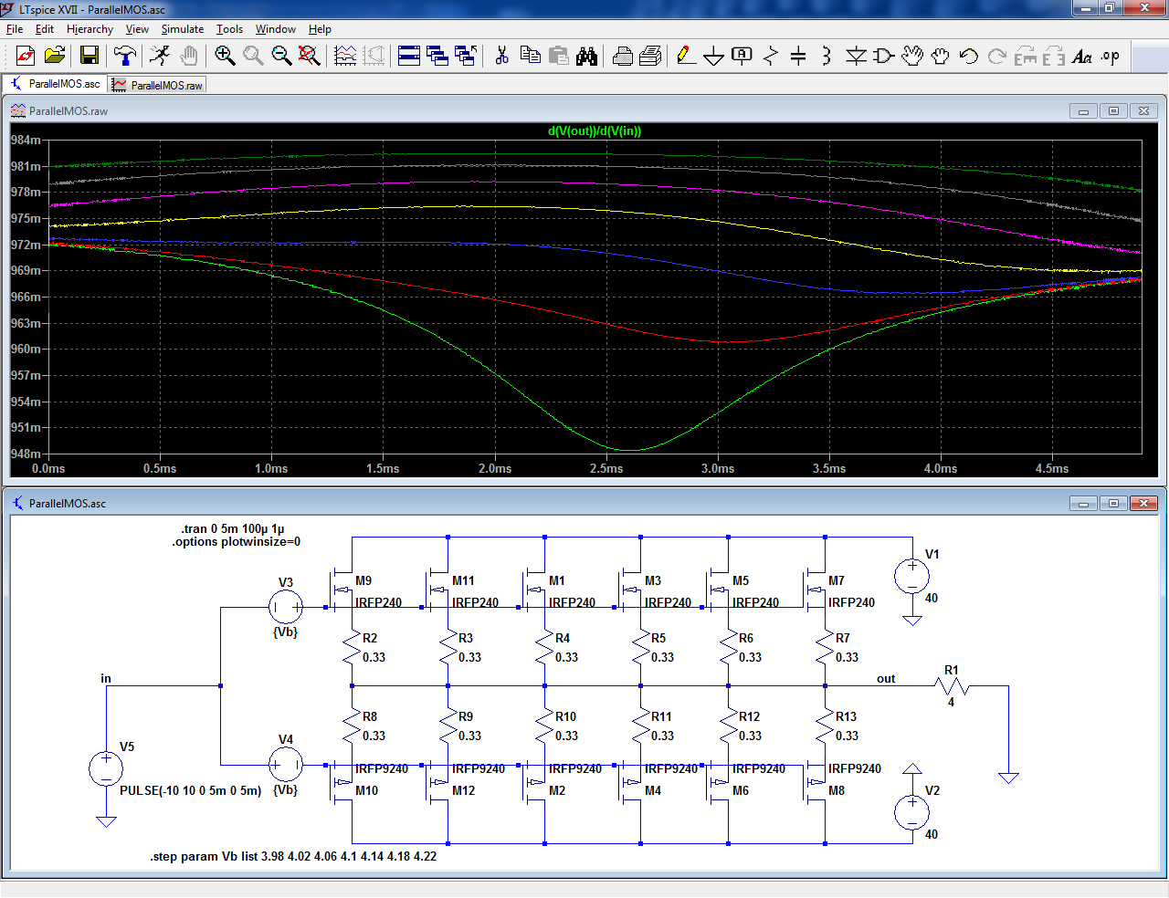
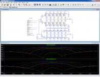
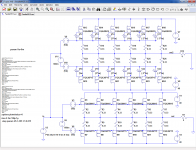
I have made the sim with the FQA's:
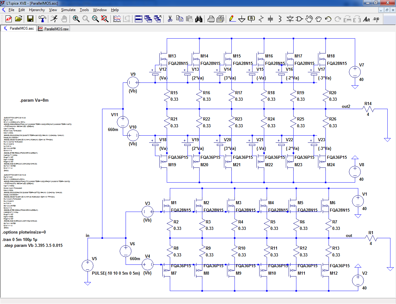
The top pane shows the situation with identical threshold voltages. This time, the transition is really ugly, maybe excessively so.
The bottom pane shows the same circuit with "random" threshold variations between -24mV and +24mV, by increments of 8mV.
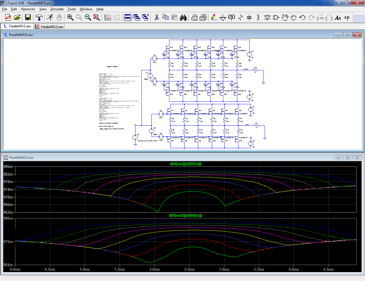
The result remains ugly, but it is obviously smoother and more civilized.
You can play with the sim, by substituting other transistors, other current steps (parameter Vb), other threshold variations (parameter Va).
Currently, the quiescent current/transistor is stepped from 24mA to 135mA.
In a real, more realistic situation, having a slight dispersion of the threshold voltages can probably help reduce the crossover artifacts.
The top pane shows the situation with identical threshold voltages. This time, the transition is really ugly, maybe excessively so.
The bottom pane shows the same circuit with "random" threshold variations between -24mV and +24mV, by increments of 8mV.
The result remains ugly, but it is obviously smoother and more civilized.
You can play with the sim, by substituting other transistors, other current steps (parameter Vb), other threshold variations (parameter Va).
Currently, the quiescent current/transistor is stepped from 24mA to 135mA.
In a real, more realistic situation, having a slight dispersion of the threshold voltages can probably help reduce the crossover artifacts.
Attachments
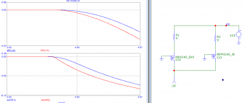
OK, that explains it. These FQA models are wrong, the real transistors don't behave like this at all.
Basically for a FET, the simple model is
Id = constant * (Vgs - Vt)^2 for Vgs >= Vt
Id = 0 for Vgs < Vt
And gm = d(Id)/d(Vgs), so
gm = 2*constant * (Vgs - Vt) for Vgs >= Vt
gm = 0 for Vgs < Vt
Below Vt, gm is zero, and above Vt, it is proportional to (Vgs-Vt). So there is a sharp corner in gm, and a discontinuity in the second derivative of gm at the point where the FET turns off.
In a real FET there is a subthreshold conduction zone where Id behaves more like an exponential, which gives a smooth transition if it occurs over a wide enough range of current. That's why IRFP9/240 and the FQA's give a smooth crossover. The laterals from ALFET don't have enough subthreshold, so they don't. And the models you got don't model it, so you get the wrong gm that looks like a "W". These models are only good for switching behavior, if you want to simulate a DC-DC converter it's fine.
Here's a comparison between EKV model and wrong model (gm on the bottom).
With LTSPICE you can use VDMOS model which fixes that, but you need the proper models that use it of course.
Attachments
Last edited:
The models are obviously wrong, but at least they show that some Vto spreading can be beneficial, even in a such an extreme and artificial situation.
The limitation of this method is that you have a finite number of transistors to parallel, and that number is generally rather small, unless you build a kilowatt monster.
I used 6 devices, which is already large, but nevertheless the spreading remains rather coarse.
It is yet another string a designer can add to his bow, and insisting on a mV-perfect matching between paralleled devices could be counter-productive.
What remains to be seen is how slight deviations from a perfect match affect the high-current sharing of the paralleled devices.
I'll make a (physical) test one of these days.
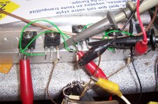
I made the parallel test.
I randomly picked 5 IRFP250 of various vintages.
I measured their Vto at 10mA and attached them to a common heatsink (non-isolated, but no thermal compound):

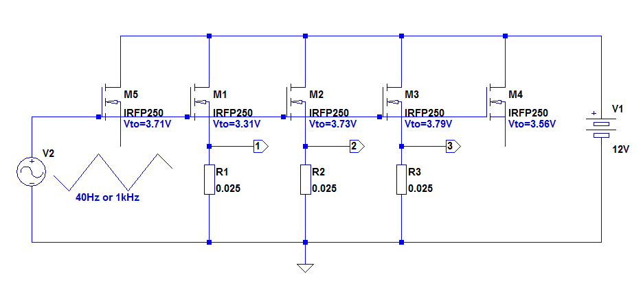
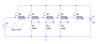
I paralleled them by triples, using a 25mΩ source resistors to monitor the currents.
The value is low enough to have a minimal effect on the current-sharing, meaning they are functionally paralleled.
I injected an offseted triangle wave into the gates (to better visualize the transconductance linearity).
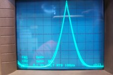
With 20mV/div (the third channel is simplified and has an external lab amp bringing it to the same level), the scale is 800mA/div, 6.4A full screen), this is the result for ~1kHz, for the three best matches (Vto=3.71V, 3.73V, 3.79V):
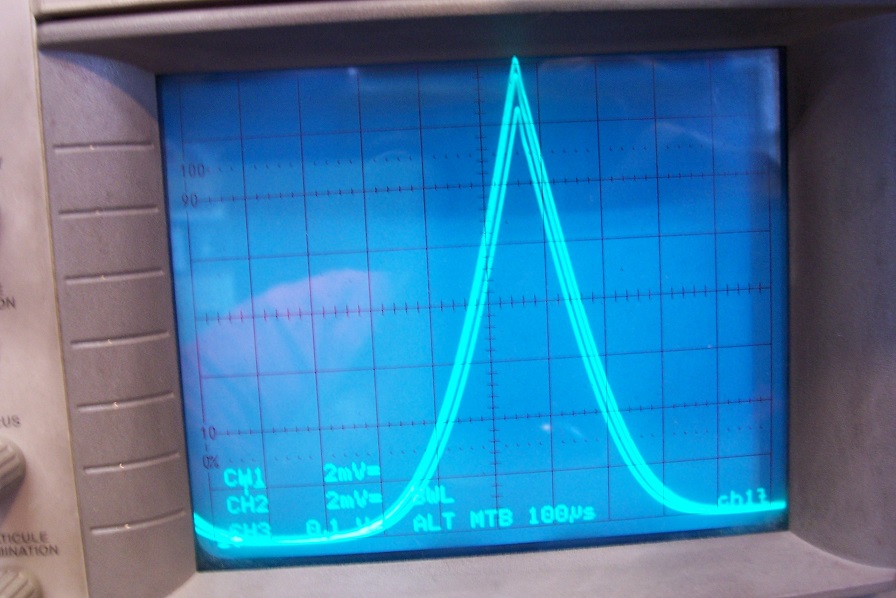
The maximum difference is 640mA, 10% thus negligible
The same with a 40Hz signal, to evaluate the effect of heating (the peak dissipation reaches 77W/device):
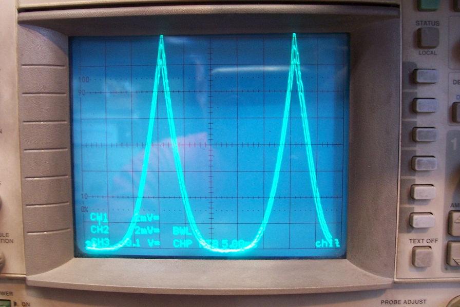
No difference (the small artifacts are caused by the digital mode of the scope)
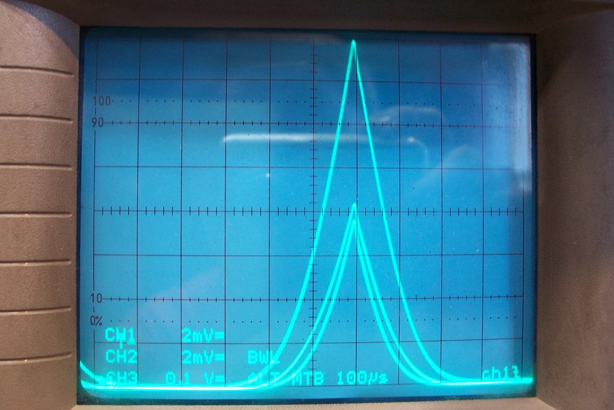
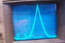
Next is two matched devices (3.71V & 3.73V) + 3.56V at 1kHz:

Somewhat paradoxically, the high-current sharing is better than for the previous case; some discrepancies are visible at a lower current.
Then at 40Hz:
No difference.
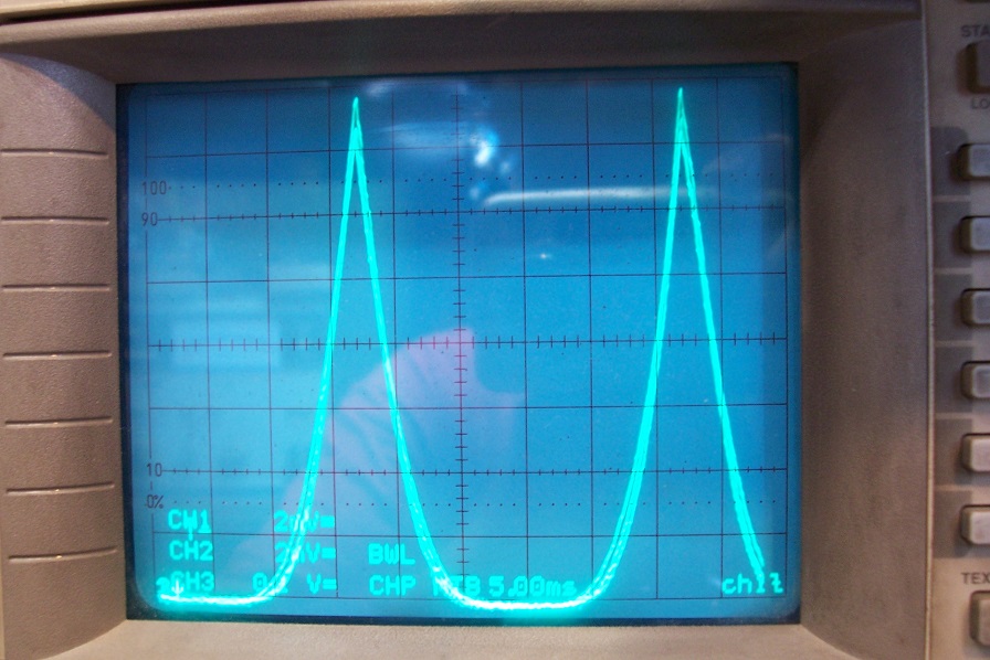
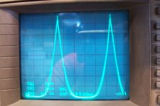
Finally, I tested the 3.31 + 3.56 + 3.73V combination at 1kHz:
This time, no miracle: with a discrepancy of >400mV in the Vto, the ratio becomes 1:2.
In summary: as long as devices are coarsely matched, the high current sharing remains perfectly OK.
Deliberately introducing small matching errors is of no consequence on the dissipation balance, and can probably improve the crossover region.
Note that the test was performed without additional balancing measures, like source resistors.
The IRFP250 are old devices, and do not have a too steep Id/Vgs curve, but more modern devices would be more demanding
I randomly picked 5 IRFP250 of various vintages.
I measured their Vto at 10mA and attached them to a common heatsink (non-isolated, but no thermal compound):
I paralleled them by triples, using a 25mΩ source resistors to monitor the currents.
The value is low enough to have a minimal effect on the current-sharing, meaning they are functionally paralleled.
I injected an offseted triangle wave into the gates (to better visualize the transconductance linearity).
With 20mV/div (the third channel is simplified and has an external lab amp bringing it to the same level), the scale is 800mA/div, 6.4A full screen), this is the result for ~1kHz, for the three best matches (Vto=3.71V, 3.73V, 3.79V):
The maximum difference is 640mA, 10% thus negligible
The same with a 40Hz signal, to evaluate the effect of heating (the peak dissipation reaches 77W/device):
No difference (the small artifacts are caused by the digital mode of the scope)
Next is two matched devices (3.71V & 3.73V) + 3.56V at 1kHz:
Somewhat paradoxically, the high-current sharing is better than for the previous case; some discrepancies are visible at a lower current.
Then at 40Hz:
No difference.
Finally, I tested the 3.31 + 3.56 + 3.73V combination at 1kHz:
This time, no miracle: with a discrepancy of >400mV in the Vto, the ratio becomes 1:2.
In summary: as long as devices are coarsely matched, the high current sharing remains perfectly OK.
Deliberately introducing small matching errors is of no consequence on the dissipation balance, and can probably improve the crossover region.
Note that the test was performed without additional balancing measures, like source resistors.
The IRFP250 are old devices, and do not have a too steep Id/Vgs curve, but more modern devices would be more demanding
Attachments


- Home
- Amplifiers
- Solid State
- ♫♪ My little cheap Circlophone© ♫♪