Wow, big change from the last PSU board post. The layout just got much more elegant. I'm very pleased =). I'm also not sure exactly why having LEDs for both power rails is important (other than for symmetry).
a little off focus, but could someone explain to me the difference between a pad connecting to a surrounding trace all around, or by four little "bridges"?
Example of all around: C5 pads on latest PCB
Example of 4 bridges: D1 pads
is there a difference? Brian i noticed you changed the type for some pads on your latest board.
Example of all around: C5 pads on latest PCB
Example of 4 bridges: D1 pads
is there a difference?
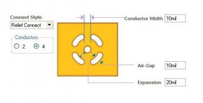
Brian i noticed you changed the type for some pads on your latest board.It's called heat relief connection, and its purpose is to aid soldering when pads are placed on large copper areas.
Without those little "bridges" you wouldn't be able to provide enough heat to allow solder fill up the hole completely, as the heat would spread into surrounding copper. This is especially critical when the copper plane is in top layer, and soldering is done through the bottom layer pad.
Removing components, with pads on large planes, is rather hard without heat relieves in place and it's very easy to damage through hole plating in such cases.
Attachments
Thanks Peter, would never have guessed... I was sure it had something to do with a better connection, but less conductor area in my mind means a worse connection...
Does this compromise sound quality? (assuming a good solder joint is obtained)
And the same note, shouldnt the pads on the diodes that are on the blue trace also be heat relieved?
Does this compromise sound quality? (assuming a good solder joint is obtained)
And the same note, shouldnt the pads on the diodes that are on the blue trace also be heat relieved?
homer09 said:Thanks Peter, would never have guessed... I was sure it had something to do with a better connection, but less conductor area in my mind means a worse connection...
Does this compromise sound quality? (assuming a good solder joint is obtained)
And the same note, shouldnt the pads on the diodes that are on the blue trace also be heat relieved?
Without the heat relief traces, it is hard to solder the components connected to the planes. The diodes can be attacked from both sides, and a good connection can be made without the relief traces.
--
Brian
homer09 said:Does this compromise sound quality? (assuming a good solder joint is obtained)
I wouldn't worry about that. It does much less damage than fuses that some designers use after the big caps 😉
Also, not properly solder filled holes (on the big caps for instance) is more trouble than those little "bridges". From what I see, Brian used 60mil connect traces on large cap relieves, which gives combined width of 240mil, which at this length (15mil) is plenty.
Hi Brian,
I would like to question one thing. Forgive me if this has been run through before long ago, but I always wondered with the LM3875 boards you made, and now this new board, why the grounds from the V+ and V- rails are not connected to each other on the PSU board itself to form one ground plane? You'd then need to move the chassis ground connection point to the PSU board.
This is how I have my P2P stereo amp wired - with local stars at each channel and then a single heavy wire from each channel star ground back to the ground plane at the PSU (and connected there at points very close to each other.) I have no hum and this is using unshielded wire everywhere and all the circuitry is out in the open - just a board for a chassis.
It just seems that the way the connections are currently made that there is a potential for ground problems in a stereo amp sharing one PSU board.
Again, apologies if this has all been hashed out before.
Jeff
BrianGT said:Here is a revised power supply board. Any comments?
--
Brian
That's more like what I was suggesting you since the beginning, Brian.
Thick, straight traces, on the same layer.
Better.😎
There might be just enough room to squeeze in several uF of X7R or Y5U surface mount capacitor between pins 1 & 4 right at the pads, actually underneath the pins that bend forward to the front row. Not as good as bypassing from both pins to ground, but that's too far away anyway. This is about as short as you will get.
Edit -> also, don't be afraid to go nuts on the size of the trace leading to pin 4 , even perhaps pour a polygon plane to there because the CMRR of the negative rail is not as good as the positive rail so it needs all the help it can get.
Edit -> also, don't be afraid to go nuts on the size of the trace leading to pin 4 , even perhaps pour a polygon plane to there because the CMRR of the negative rail is not as good as the positive rail so it needs all the help it can get.
The link to the wiki in post #62 doesn't work.
Or is it just me? This is what happens:
Very nice PSU. I like those fat traces🙂
Steen.
Or is it just me? This is what happens:
Invalid page name.
Very nice PSU. I like those fat traces🙂
Steen.
jeff mai said:...with local stars at each channel and then a single heavy wire from each channel star ground back to the ground plane at the PSU (and connected there at points very close to each other.)
Yes, that's how I do it too.
Guys, you should forget the Gaincard once and for all.😎
I have always used "local stars at each channel and then a single heavy wire from each channel star ground back to the ground plane" on my amps and obviously it has worked well as it is the standard way of doing it, but I have to admit that my BrianGT GC doesn't have any obvious problem wired up with a star on each amp pcb. It is quiet.
I have a "gut feeling" that two pairs of twisted wires from the psu pcb and amp psu may actually be better at cancelling noise than twisting the +ve and -ve wires and having a separate earth wire. I haven't proven it one way or the other. So what do others think?
I have a "gut feeling" that two pairs of twisted wires from the psu pcb and amp psu may actually be better at cancelling noise than twisting the +ve and -ve wires and having a separate earth wire. I haven't proven it one way or the other. So what do others think?
The pcb set is almost finalized, and I should be able to order a batch of boards today.
I put up a new kit page on my website:
http://www.chipamp.com
(click on LM3886 kit in the left column)
I will start accepting pre-orders relatively soon, once I order the pcbs.
--
Brian
I put up a new kit page on my website:
http://www.chipamp.com
(click on LM3886 kit in the left column)
I will start accepting pre-orders relatively soon, once I order the pcbs.
--
Brian
RIFA electrolytic application guide
Brian,
I attach a RIFA electrolytic application guide page 5.
It seems the way you do the trace on previous PS board (lm3886-combined.gif), by having two layers (1 for + and 1 for -) seems to be a better approach to lower the inductance of the circuit.
http://www.evox-rifa.com/electrolytic_cat/electrolytic_appguide.pdf
Regards,
---
David
Attachments
Re: RIFA electrolytic application guide
Given that we only have a single large capacitor, it seems like it would work out just fine having both traces on the bottom layer, and avoiding having overlapping tracks.
Also, with the large planes, it will be easier to solder the capacitors if the planes are on the bottom of the pcb, as the soldering iron will make contact with the plane, and not just the plated through hole. I feel that the copper area is big enough. Of importance also is obtaining a good soldering joint, and reducing the possibility of a cold solder joint. I don't see this as much of a problem on the amplifier board and the planes on the top layer, so I am leaving it as is.
--
Brian
dw1narso said:Brian,
I attach a RIFA electrolytic application guide page 5.
It seems the way you do the trace on previous PS board (lm3886-combined.gif), by having two layers (1 for + and 1 for -) seems to be a better approach to lower the inductance of the circuit.
http://www.evox-rifa.com/electrolytic_cat/electrolytic_appguide.pdf
Regards,
---
David
Given that we only have a single large capacitor, it seems like it would work out just fine having both traces on the bottom layer, and avoiding having overlapping tracks.
Also, with the large planes, it will be easier to solder the capacitors if the planes are on the bottom of the pcb, as the soldering iron will make contact with the plane, and not just the plated through hole. I feel that the copper area is big enough. Of importance also is obtaining a good soldering joint, and reducing the possibility of a cold solder joint. I don't see this as much of a problem on the amplifier board and the planes on the top layer, so I am leaving it as is.
--
Brian
site is working again (MCI had routing issues this morning and it was down).
Parts list and info on the webpage:
www.chipamp.com
I will post pricing information start accepting pre-orders soon.
--
Brian
Parts list and info on the webpage:
www.chipamp.com
I will post pricing information start accepting pre-orders soon.
--
Brian
So, to be clear, even if we've signed the WIKI in order to actually get our kits we'll have to place the order on Chipamp.com correct?
m0tion said:So, to be clear, even if we've signed the WIKI in order to actually get our kits we'll have to place the order on Chipamp.com correct?
Yes, the Wiki was just to get an idea if people were interested in pcbs and kits, so that I can gauge the interest before I decide to order kits, and give me an idea of what to set for pricing (parts are cheaper in large quantities).
I will put up the order page soon, and remove the Wiki (have it direct to the order page).
--
Brian
- Home
- Amplifiers
- Chip Amps
- my first try at a LM3886 layout, any comments/suggestions?