Abetir, I tried to not change too much of your original designed here.
This is my modification.
Using CFP reduce slew rate, I do not know how to increase the slew rate. May be using higher VAS current with capable transistor like 2SC3053 can increase the slew rate a bit.
I simplified Symasym amplifier, have almost same result but much higher slew rate and it tested by my friends.
Attachments
Abetir, I tried to not change too much of your original designed here.
This is my modification.
Using CFP reduce slew rate, I do not know how to increase the slew rate. May be using higher VAS current with capable transistor like 2SC3053 can increase the slew rate a bit.
I simplified Symasym amplifier, have almost same result but much higher slew rate and it tested by my friends.
Bimo,
Thank you! will check this out tonight...

Meanwhile...I think I was able to straighten a few things in the design...but the extracted open loop gain is rather confusing...hope I did it right in sim.🙂
Attachments
Hi,
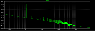
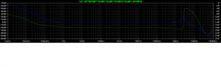
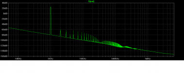
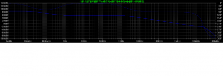
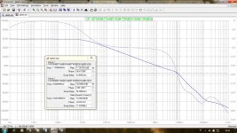
bimo, I don´t get sensible results for the OL-simulation with Your file.
CL-simulation gives ~30dB gain as expected.
jauu
Calvin
bimo, I don´t get sensible results for the OL-simulation with Your file.
CL-simulation gives ~30dB gain as expected.
jauu
Calvin
Last edited:
Calvin,
This is my results following bimo's mod...it looks interesting neatier than my work....i just don't know how to probe it..😛
Bimo,
I think I can patch your changes in the actual pcb. I'll give it a go just for a test. 😉
This is my results following bimo's mod...it looks interesting neatier than my work....i just don't know how to probe it..😛
Bimo,
I think I can patch your changes in the actual pcb. I'll give it a go just for a test. 😉
Attachments
Calvin,
This is my results following bimo's mod...it looks interesting neatier than my work....i just don't know how to probe it..😛
Bimo,
I think I can patch your changes in the actual pcb. I'll give it a go just for a test. 😉
You should read this thread.
I believe it discuss how to use Tian probe to calculate phase margin and gain margin. I learned it from Dadod and Bonsai.
For 2SC4793, 2SA1837, 2SA1943, and 2SC5200, I use Keantoken model. If posible please use Bob Cordells model and Keantoken models.
Please don't chase slew rate. Go for a low overall thd *combined* with low high order harmonics.
Its really about the music.
Use your test equipment and listening auditions with friends.
-bruce
Its really about the music.
Use your test equipment and listening auditions with friends.
-bruce

Hi,
bimo, I do know the Tian probing ... guess who´m the schematic of #38 is of? ;-)
With Your file from #51, when I set V3 to AC=0, activated the ";.step param prb list -1 1" line, deactivated ".param prb=0" line and run the AC sim, plotting the "-1/(1-1/(2*(I(Vi)@1*V(x)@2-V(x)@1*I(Vi)@2)+V(x)@1+I(Vi)@2))" line, the result is a amplitude response at ~26dB with a bandwidth of just over 10kHz.
Could You tell what You did instead?
jauu
Calvin
I'm quite sure that "CFP" means the use of Sziklai pairs in the amplifier output. It's an abbreviation - for what? Googling didn't help either, as it's prime result was Certified Financial Planner. To good to be true, isn't it 🙂?
Best regards!
Best regards!
Last edited:
Bimo and others the new mod works right on at power switch!. 
Amp is still pretty silent no hum no thump no oscillation happened. As Im still using the same board I had to do minor changes in component values to suit the same devices per my first build and only allow changes according to the present pcb size. Believe me I did surgical operation 😀
The are, 100r collector driver resistor, added degenerators 2r2 for drivers 15r for VAS ltp and 47r for the input diff, cannot accomodate phase lead cap 5p6 [not installed] instead put 3p3 across 10k of feedback resistor, 20k to input current source referenced to ground. omitted temporarily 1r damping resistor.Everything else was untouched.
Sonic is very good the details is complete and transparent.
I will revise the pcb to accomodate all the changes per bimo's schematic and Valery's recommendation of replacing VAS devices to the larger TO-126. I imagine with all of these changes the circuit will become more robust with an improved stability margin.

Allbert
Amp is still pretty silent no hum no thump no oscillation happened. As Im still using the same board I had to do minor changes in component values to suit the same devices per my first build and only allow changes according to the present pcb size. Believe me I did surgical operation 😀
The are, 100r collector driver resistor, added degenerators 2r2 for drivers 15r for VAS ltp and 47r for the input diff, cannot accomodate phase lead cap 5p6 [not installed] instead put 3p3 across 10k of feedback resistor, 20k to input current source referenced to ground. omitted temporarily 1r damping resistor.Everything else was untouched.
Sonic is very good the details is complete and transparent.
I will revise the pcb to accomodate all the changes per bimo's schematic and Valery's recommendation of replacing VAS devices to the larger TO-126. I imagine with all of these changes the circuit will become more robust with an improved stability margin.
Allbert
Hi,
bimo, I do know the Tian probing ... guess who´m the schematic of #38 is of? ;-)
With Your file from #51, when I set V3 to AC=0, activated the ";.step param prb list -1 1" line, deactivated ".param prb=0" line and run the AC sim, plotting the "-1/(1-1/(2*(I(Vi)@1*V(x)@2-V(x)@1*I(Vi)@2)+V(x)@1+I(Vi)@2))" line, the result is a amplitude response at ~26dB with a bandwidth of just over 10kHz.
Could You tell what You did instead?
jauu
Calvin
Please set all V1, V2, and V3 AC=0.
Sonic is very good the details is complete and transparent.
Allbert
Congratulation...
Please share the schematic.
Schematic attached per my latest build.
bimo,
Can you teach me how to calculate the slew rate in the schematic? I know how to place the probes in the slope, but I could'nt bring the output transient to triangle like. At what amplitude and freq should I have it set?
By rough calculation,
SR=Icmax/C
then,
1500÷33=45.454
where Icmax is first input transistor collector current and C is Vas miller comp cap.
Regards,
Albert
Attachments
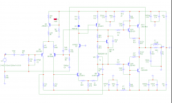
I'm quite sure that "CFP" means the use of Sziklai pairs in the amplifier output. It's an abbreviation - for what? Googling didn't help either, as it's prime result was Certified Financial Planner. To good to be true, isn't it 🙂?
Best regards!
Hi kay,
In electronics, the Sziklai pair (also known as a complementary feedback pair (CFP) or "compound transistor"...
..according to Wikipedia. 😉
Regards,
Albert
Thanks, abetir 😎!
Btw, your schematics look very promising. Most probably I'll try it at a rework of a former quasi-complementary amplifier pair from the early 1970ies.
Btw, where did you attach the Vbe multiplier transistor Q6 to? To the dirvers, or to the output devices, or to both?
Best regards!
Btw, your schematics look very promising. Most probably I'll try it at a rework of a former quasi-complementary amplifier pair from the early 1970ies.
Btw, where did you attach the Vbe multiplier transistor Q6 to? To the dirvers, or to the output devices, or to both?
Best regards!
Hi kay,
The prototype pcb lay-out is in post #34 [to be updated soon] you may notice the VBE transistor is in line with both +-drivers so that a common heatsink can be installed. My knowledge was that, to get the best thermal tracking behaviour of the VBE transistor a better implementation is to group them tightly with the drivers. Output devices are separately mounted on the main heatsink.
Regards!
Folks,
Anyone care to shed light on the purpose of the LEDs in the attached image? The common base cascode in the balanced VAS is a current error sensor yet this one the base is clamped to minus rail with 3 diodes. This is from one of the late Dr. Bora's VAS design.
Sa Muli,
Albert
Anyone care to shed light on the purpose of the LEDs in the attached image? The common base cascode in the balanced VAS is a current error sensor yet this one the base is clamped to minus rail with 3 diodes. This is from one of the late Dr. Bora's VAS design.
Sa Muli,
Albert
Attachments

Folks,
Anyone care to shed light on the purpose of the LEDs in the attached image? The common base cascode in the balanced VAS is a current error sensor yet this one the base is clamped to minus rail with 3 diodes. This is from one of the late Dr. Bora's VAS design.
Sa Muli,
Albert
The LED for voltage reference (similar to zener diode).
- Status
- Not open for further replies.
- Home
- Amplifiers
- Solid State
- My CFP design, need your help!