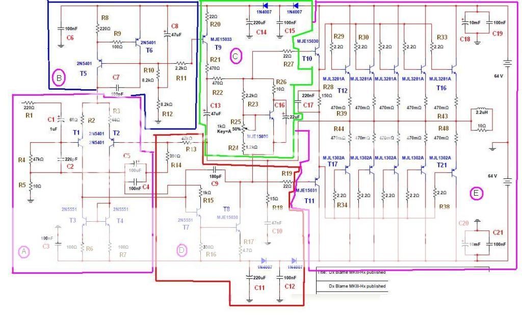
Can you post a better diagram with voltages, at my age I can't read the one posted above in post88!
Left click to enlarge image, then right click on image and select view image. On new page click again to enlarge. If you still can't read it, hold Ctrl and hit the "+" sign.
😉
Member
Joined 2009
Paid Member
that works !
I'm not seeing what is wrong with this amplifier. Like Ian, I would say that 2mA through R18 is fine, it provides plenty of drive for the VAS, although 1mA is also OK but this is fine tuning that probably isn't necessary. If R18 is hot then something funny is going on. If R18 is only seeing 2mA through 330R then it can not be self-heating. Is it possible that it is being heated via conduction from something else nearby - are the other parts nearby also hot ?
I'm not seeing what is wrong with this amplifier. Like Ian, I would say that 2mA through R18 is fine, it provides plenty of drive for the VAS, although 1mA is also OK but this is fine tuning that probably isn't necessary. If R18 is hot then something funny is going on. If R18 is only seeing 2mA through 330R then it can not be self-heating. Is it possible that it is being heated via conduction from something else nearby - are the other parts nearby also hot ?
Hi guys
R18 is not hot - it's cool to the touch as is the VAS driver transistor. I think the problem here is simply a gross mismatch between the PNP and NPN drivers, as Andrew alluded, and a mismatch between the output pairs.
But it plays music and sounds rather good when hooked up to a decent speaker.
Ian, thanks very much for that link - some good ideas particularly for the R values.
i never found your isues as a problem....really...😉
as mentioned earlier the circuit taken as whole will reach thermal equilibrium.....
and because it is a closed loop, feedback takes care that the quiescent
operating points are maintained...
the universal criteria on output offset voltage, and the fact that you can adjust
your output trannie's idle current thru the vbe multiplier is proof enough
that you have a viable working amp, anything else is a bonus....
i do not see any point to making R18 330 ohms,
lower resistance mean more current drain,
current that the VAS can better use...
3,3k for R18 is better...
as mentioned earlier the circuit taken as whole will reach thermal equilibrium.....
and because it is a closed loop, feedback takes care that the quiescent
operating points are maintained...
the universal criteria on output offset voltage, and the fact that you can adjust
your output trannie's idle current thru the vbe multiplier is proof enough
that you have a viable working amp, anything else is a bonus....
R18 is not hot
i do not see any point to making R18 330 ohms,
lower resistance mean more current drain,
current that the VAS can better use...
3,3k for R18 is better...
Hi
OK, I'm confused by a few part references here, but then I haven't been reading for long, nor looked at errors. Regarding R18 then, what did mean by post #88?
On more usual stuff, the VAS buffer (Q9) collector is grounded in every example I've seen, Bob Cordell's too. Bob though, does use lower values like 470R for the emitter load (R18). Doug uses a nominal 2k. I take it that ground is a better reference point and the bias current is a matter of experiment or theory for lower distortion. I've just put down Self's latest tome on the subject after a couple of hours read and though I think I've grasped a little more, I'm probably none the wiser there. Even he admits to design problems with poor or rather too generic SPICE models of suitable small transistors as much as anyone else. With LT or any sim. package, you are still at the mercy of some crummy, misleading data somewhere.
This EF type of design is as not as easy to follow as it looks either and it seems to have been developed iteratively over decades. Much effort with Sam Groner's input to the new book has gone into transistor types and simulation but no mention is made of DIYAudio staples like the last remaining Fairchild CRT driver transitors used in the VAS, even though low Cob or Cbc is.
OK, I'm confused by a few part references here, but then I haven't been reading for long, nor looked at errors. Regarding R18 then, what did mean by post #88?
If you meant R35 which would be in context, I can believe that. I think 180-220R is usual there.Attached is the voltage overlay with this new board with 3pr outputs on 56V rails and 50R between the driver emitters. R18 dissipation is extremely high!
On more usual stuff, the VAS buffer (Q9) collector is grounded in every example I've seen, Bob Cordell's too. Bob though, does use lower values like 470R for the emitter load (R18). Doug uses a nominal 2k. I take it that ground is a better reference point and the bias current is a matter of experiment or theory for lower distortion. I've just put down Self's latest tome on the subject after a couple of hours read and though I think I've grasped a little more, I'm probably none the wiser there. Even he admits to design problems with poor or rather too generic SPICE models of suitable small transistors as much as anyone else. With LT or any sim. package, you are still at the mercy of some crummy, misleading data somewhere.
This EF type of design is as not as easy to follow as it looks either and it seems to have been developed iteratively over decades. Much effort with Sam Groner's input to the new book has gone into transistor types and simulation but no mention is made of DIYAudio staples like the last remaining Fairchild CRT driver transitors used in the VAS, even though low Cob or Cbc is.
DIYAudio staples like the last remaining Fairchild CRT driver transitors used in the VAS, even though low Cob or Cbc is.
the crt boards of most color tv's and pc monitors are a good source of these tranies,
i collect those as well....
a board gets you a VAS pair to use and one spare trannie....😀
Thanks everyone for your replies.
Ian, my post #88 was poorly worded; R18 dissipation is not high (it is cool to touch) but the current draw is higher than expected.
I do believe that the imbalance is largely due to mismatch of the PNP and NPN drivers (and to a lesser extent outputs...). As AJT says its probably not a big problem and both amplifier boards sound fine.
I'd like to think I can do better though and have been researching driver alternatives. I've lost confidence in the On Semi MJE1503x devices, having tested a number of devices finding the PNP and NPN pairs are not even remotely close. These are genuine transistors sourced directly through On Semi's samples programme.
If I can source the 2sa1837/2sc4793 then I will give those a go instead. Thoughts?
After studying the Tag McLaren schematic I'm considering a few other component changes:
R18: 330R -> 2k2
R19: 10R -> 56R
R35 may increase from 100R to 150R or 180R.
If I can source the 2sa1837/2sc4793 then I will give those a go instead. Thoughts?
you will get the same results, so i say let it go.....
unless you have a distortion meter you can use to
determine if thd improved with the change...
After studying the Tag McLaren schematic I'm considering a few other component changes:
R18: 330R -> 2k2
R19: 10R -> 56R
R35 may increase from 100R to 150R or 180R.
just watch out for the output offset voltages though...
my take...
if you want more current thru your VAS,
change R12 to 56 ohms from 100 ohms,
R19 to 5.6 ohms from 10 ohms...
R18 can be 1k instead...
i will just leave it as it is if you are not having other heat and sonic issues....😉
congratulations on you first design and build....
i have a system of looking at circuits, as long as hFE of trannies
are >> than 10, then you can assume the collector current is equal to
emitter current, what this means is that you don't look at base currents,
specially easy for small signal analysis...
exception would be the output stage emitter followers, where you really have to consider
hFE, and even here, if current gain is very very high, then input base current is not relevant....
VAS current will be very very high compared to EF input current you can ignore it...
if you can see this picture in your head, then you can look at different circuits with ease...
2SC4793/A1837 were very fine drivers but look at the maximum current rating - 1 amp!
MJE150XX series drivers are virtual output transistors rated for up to 8 amp.
With a 3 pairs of EF output transistors working at the rated capability, the Toshibas will run
out of breath, even if they do sound fine with normal domestic levels of only 1-5W.
If you design a massive amplifier, there's no point strangling it with dinky drivers so the parts are probably going to best left with MJE series for 3 pairs, as total current is much more than a single pair, where the Toshiba parts would otherwise excel.
We often talk about transistor maximum current and gain figures as if they were true at all load conditions but old power transistors in particular, fall off rapidly from about 70 down to 10-20 Hfe when they are are asked to crank out their rated power above an amp or so, into low impedance like, 4R loads. That's why the real amplifiers designed to power crazy 1R electrostatic speaker impedances and party hook-ups are built with EF triples with scads of gain, just to allow for their woeful performance when the heat is on.
Modern power transistors like the landmark 2SC3281/A1302 family of parts (MJL3281/1302 etc.) are much better at low beta droop as this property is known. The transistors still require increasing proportions of base current V emitter current when they begin to work at higher than ~5 amps, though - just nowhere near as bad as say 2N3055 or 2N3773.
'Plenty more on this and designing any stage you like in Bob and Douglas's books. If you like designing, then spend plenty of time absorbing these books, if you haven't already begun to. 🙂
All good points, gentlemen. It's working well so I'll leave it alone.
I'm going to increase R18 to 1k and then finish the chassis. I've got a nice aluminium case with big heatsinks and a pair of 40V / 300VA transformers. This will be my first dual mono build
I'm going to increase R18 to 1k and then finish the chassis. I've got a nice aluminium case with big heatsinks and a pair of 40V / 300VA transformers. This will be my first dual mono build
Hey Patrick,
Did you also build a stock MKIII? I'd like to know how they compare.
Thanks, Terry
Did you also build a stock MKIII? I'd like to know how they compare.
Thanks, Terry
Yes I built a stock MkIII about 6 months ago and was very pleased with the result. This design presented here has almost identical topology, the difference being removal of the VAS bootstrap and simplification of the Vbe - I don't really understand why Carlos had a couple extra R's in his - I jumpered them out on these boards. Possibly to do with the hybrid CCS/bootstrap load.
Other than that the R and C values have been 'optimised' to my liking (translation: I read Cordell and Self and applied their recommendations). The input RC filter has been properly worked out, the NFB cap enlarged significantly, and is more in line with Kevin's LTT4 design in that respect.
I would have liked to cascode the LTP current mirror and adopt an EF3 output stage. These changes to the topology would necessitate a new board and I don't have the skills to do that yet.
The other obvious change is to the output stage: 3pr down from 5pr. Rail voltage and gain reduced accordingly. I don't really need another 250w amplifier, nor do I need enormous current capability for my fairly well behaved 8R loudspeakers. As it stands, 3pr of these 230W devices is probably overkill.
Terry, I will let you know (probably via PM) my thoughts after I've spent time listening to it and comparisons to the MkIII. I'm not really expecting much: any differences will probably be as a result of the bootstrap and differences in the power supply / grounding.
If you want 'ultimate Blameless' then you probably need look no further than OStripper's Wolverine v1.2 coupled to the Slewmaster board. It's got all the bells and whistles and all the values have been worked out in sim.
But if you are chasing a sound then have a talk to Bigun. This guy knows how to voice an amp and his TGM8 is the one I reach for most times.
Hi Patrick,
Thanks for the explanation. Very helpful. FYI, Kevin now has a pair of boards thanks to Jason and I have asked him to build at least one of them in order to determine what is amiss. It will be interesting to see how it compares to yours when things are finally resolved.
I don't need any more 250W amps either. I have mainly built the ones I have because I have/had transformers for them. I have Slewmonster boards coming and hopefully will try a few different topologies with them.
My DX MKIII sounds almost identical to my DX Super A. I find myself reaching for the DX Super A much of the time. It seems easier to sweeten the sound of a mid voltage amp than HV. Maybe that is just my findings.
Without wanting to spoil the party (and I agree that a successful design exercise is time for a celebration  ) I think you should investigate the amplifier's capabilities by demonstrating, perhaps only for your satisfaction, that it does more than say a 10W amplifier can.
Build yourself some 100W+ dummy loads from wire-wound power transistors (you can use large values like 100R in parallel to cancel inductance) or splash out on a few metal-clad 50W resistors and surplus heatsinks to make yourself something that will last for all designs and experiments. This is the crunch test for amplifiers - if you don't do it, you really never know what lurks in your design and it's capabilities are only notional. I had a couple of 100W amplifiers returned for refund when a repair technician commented that one 100W design didn't make it past 75W before it began to show instability with a 10kHz tone. This was a sad time for me but it is only one of the major differences between DIY and commercial products.
Bite your lip and do it, using a controlled amount of standard input tones and look at the output with a 'scope or suitably interfaced USB soundcard or a decent native one in your PC. Bear in mind that testing to the limits of your design could mean disaster when you test for what the nominal power rating really means. Start with low input levels and observe any anomalies like even minor oscillation using 100,1k,10kHz tones, as you increase power in steps like 1,5,10,20W...and so on.
I have to do this kind of testing with every repair of PA and musical instrument amps and recycled audio relics that musos and DIYs have brought to me when they can't fix it. It's obviously necessary for anything sold, like one of my own designs or a recycle. Maybe I don't often do it to the max. power rating but unless you test power capability, the dream may remain just a dream.
The need for some form of power testing is clear though - no less than testing that a car accelerates and stops like it should and the adverts say.
) I think you should investigate the amplifier's capabilities by demonstrating, perhaps only for your satisfaction, that it does more than say a 10W amplifier can.Build yourself some 100W+ dummy loads from wire-wound power transistors (you can use large values like 100R in parallel to cancel inductance) or splash out on a few metal-clad 50W resistors and surplus heatsinks to make yourself something that will last for all designs and experiments. This is the crunch test for amplifiers - if you don't do it, you really never know what lurks in your design and it's capabilities are only notional. I had a couple of 100W amplifiers returned for refund when a repair technician commented that one 100W design didn't make it past 75W before it began to show instability with a 10kHz tone. This was a sad time for me but it is only one of the major differences between DIY and commercial products.
Bite your lip and do it, using a controlled amount of standard input tones and look at the output with a 'scope or suitably interfaced USB soundcard or a decent native one in your PC. Bear in mind that testing to the limits of your design could mean disaster when you test for what the nominal power rating really means. Start with low input levels and observe any anomalies like even minor oscillation using 100,1k,10kHz tones, as you increase power in steps like 1,5,10,20W...and so on.
I have to do this kind of testing with every repair of PA and musical instrument amps and recycled audio relics that musos and DIYs have brought to me when they can't fix it. It's obviously necessary for anything sold, like one of my own designs or a recycle. Maybe I don't often do it to the max. power rating but unless you test power capability, the dream may remain just a dream.
The need for some form of power testing is clear though - no less than testing that a car accelerates and stops like it should and the adverts say.
Last edited:
Which R's were you referring to? This seems to be the last official schematic :....I don't really understand why Carlos had a couple extra R's in his - I jumpered them out on these boards. Possibly to do with the hybrid CCS/bootstrap load....
An externally hosted image should be here but it was not working when we last tested it.
But the part numbers may be here, I think.
Re post #116:
That is excellent advice and I will certainly conduct some stress testing. I will be placing an order with Digikey in the near future and will purchase some power resistors. Would two of these 8R resistors be suitable? My thoughts were I could use a single resistor to determine the max power into rated load and then two resistors in parallel to stress test. Is 4R resistive load an adequate test for a 8R amp? AndrewT suggests 2R6 but most others here seem to test with only 8R.
I'll research PC Card interfacing.
Invalid Request
DX BLAME III, R21,22 are fair enough to drop, as they are for a mid-point tap for the bootstrap reference.
R26 though, is presumably to correct for non-linearity or simply the coefficient in mV/degree K or whatever, of the Vbe bias compensation.
As you refer to Self, have a look at his chapter on thermal compensation. In the latest edition, it's R3 in chap. 22 p532 ff and in the 5th edition, it's chap. 15 p412 ff. It's there in all editions though.
'Quite serious stuff, that thermal compensation, as it impacts on distortion too. I'd think about that before dismissing the idea or the resistor.
Power resistors
Those traditional type power resistors for freestanding air cooling are a tad expensive in high power ratings these days. This is the more normal option with any big heatsinks or blocks of aluminium you can find - it doesn't have to look nice, so use what you find free etc: Invalid Request
The recognized load for proving amps is 8R. Lower resistances certainly give the amplifier a harder time but the best asset is separate load resistor units like 4 x 50W 8R resistors, each on separate sinks for roughly 50W dissipation. That gives the options of 4 x 8R 50W, 2x 4R 100W, 1x 8R 200W 1 x 2R 200W and so on.
Because they were cheap, I bought a bag of 100 x 100R 5W ceramic block resistors years ago and when many are paralleled, these show no effect of parasitic inductance. They get hot without heatsinking, so they don't just lie on the bench but either hung out of the window or dropped in a bucket of water alongside for protracted testing. Short tests require very little heatsinking. 'Sinks of around 1 degree/watt are adequate for most short term use with 50W resistors and these are quite cheap and common.
Measurements.
Pete Millet's soundcard interface is a masterpiece and still here in the test equipment forum and available on Ebay as a kit of PCB, front panel and instructions but I couldn't easily buy the precise plastic case for it. I have built Silicon Chip's simpler versions in the past, since this is not rocket science but last time I looked, there were many basic OPamp + attenuator switch projects on the net but few offered proper limiting or clipping of the input to prevent anything over 2V peak from frying your card.
Ultimate precision is not necessary for 'scoping the power output but some way of protecting the vulnerable input stage of soundcards from overdrive is, absolutely.
Last edited:
- Status
- Not open for further replies.
- Home
- Amplifiers
- Solid State
- My Blameless