Hi all
I've been interested in the Linn/Blameless topology for a while and wanted to try my hand "designing" one of these.
I've got some spare DX Blame MkIII amplifier board from the last group buy and thought I'd have a go at selecting my own component values that will result in a "reference design" that is entirely conventional in every respect. The schematic is based on what I've learnt from reading Cordell and Self, and what I've seen from the DIY projects here - notably the DX designs from Carlos and Kevin's recent LTT4 project.
The MkIII boards support:
- LTP input stage with currrent mirror and cascoded CCS
- EF2 output stage
I know this will bore seasoned members here; however, I would really appreciate your advice in fine tuning the C and R values.
thanks
Attachments
Last edited:
Looks like a good thread waiting to happen, there's a lot to be said for a reference, conventional design
Hi Christian,
Watching with great interest. Be sure to check out the end of the of the MKIII thread to see how to fix the lifted ground error on those boards. Wishing you great success with this.
Blessings, Terry
Watching with great interest. Be sure to check out the end of the of the MKIII thread to see how to fix the lifted ground error on those boards. Wishing you great success with this.
Blessings, Terry
Thanks Terry - will do. I remember following your progress in the Builders Thead several months ago - I've got in my bookmarks to follow up on.
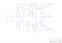
The Input 1uF DC blocker is in the wrong place.
It must go before the 47k.
Or move the 47k to after the 1uF.
R16 is tapped into the wrong end of R14.
The collector of Q10 drives the base stopper.
Reduce R13 to <=1k5
You have too much Vbias available with 2k2. Depending on actual Vbe of the transistors, you might find you can bias the output using just 1k0 or 1k1 for R13
R17 is far too high.
Try 1k0 to 2k0.
Add an output Zobel.
R10 is fed from the -ve rail, try increasing it's value substantially, or move it to Power Ground.
Last edited:
yes, the base of the left hand side of the ltp needs to be properly dc biased,
otherwise huge offset voltage at the output....
otherwise huge offset voltage at the output....
Thanks everyone - I will make the changes to the schematic tonight.
The boards I'm using can accomodate one or two diodes strings (or resistors) on the rails between the driver and front end. However most designs I've seen here and in books have nothing. Would there be benefit in using them?
Also there are a couple of extra locations for power supply decoupling (HF). Again in most of the Linn/Blameless designs they aren't used.
Attachments
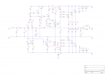
VR in the multiplier is on the wrong leg.
These next three are my preferences.
I would allow for a link between Signal Ground and Power Ground.
Locate in the ground trace between the tappings for C6 & R10.
This link may have to pass some Fault Current from a faulty Source. So allow for Power Diodes in inverse parallel as well as the low value resistor.
I would also add more on board Decoupling.
The input transistors are 2n type.
The lead outs of BCxxx and 2sc/axxxx are different. What about a 4th pad to allow other transistors to be fitted?
Last edited:
Maybe add some RC filtering on the power rails between the output transistors and the rest of the circuit? And then a second RC filter between the VAS and the input LTP?
I'm a bit of a power rail freak. Whenever I have films and electrolytics paralleled I add a snubber across them. (1R + 1u). Some may disagree with this approach...
I'm a bit of a power rail freak. Whenever I have films and electrolytics paralleled I add a snubber across them. (1R + 1u). Some may disagree with this approach...
Last edited:
VR in the multiplier is on the wrong leg.
These next three are my preferences.
I would allow for a link between Signal Ground and Power Ground.
Locate in the ground trace between the tappings for C6 & R10.
This link may have to pass some Fault Current from a faulty Source. So allow for Power Diodes in inverse parallel as well as the low value resistor.
I would also add more on board Decoupling.
The input transistors are 2n type.
The lead outs of BCxxx and 2sc/axxxx are different. What about a 4th pad to allow other transistors to be fitted?
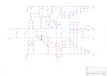
Is this what you had in mind? I can't fit extra (4th) pads because I'm working within the limitations of an existing PCB (DX Blame MkIII)
Attachments
Maybe add some RC filtering on the power rails between the output transistors and the rest of the circuit? And then a second RC filter between the VAS and the input LTP?
I'm a bit of a power rail freak. Whenever I have films and electrolytics paralleled I add a snubber across them. (1R + 1u). Some may disagree with this approach...
I could add an RC filter on the rails where the 220u caps are located, between the drivers and the VAS. What corner frequency do you suggest?

Yes, but maybe move C15 and C16 to the other side of the resistors R38 and R39 unless C15 and C16 are for the driver decoupling.
Corner frequency looks fine to me.
Can you add decoupling for each of the output transistors? So it can connect as close as possible to the output transistor collectors.
Corner frequency looks fine to me.
Can you add decoupling for each of the output transistors? So it can connect as close as possible to the output transistor collectors.
R10 and R17 should connect to signal GND.
R17, R18 are on the large side. R17 is usually 100R-220R, R18 usually 470R.
R17, R18 are on the large side. R17 is usually 100R-220R, R18 usually 470R.
That looks to me to be a workable schematic.
You could play around with component values in LTspice.
You could play around with component values in LTspice.
R10 and R17 should connect to signal GND.
R17, R18 are on the large side. R17 is usually 100R-220R, R18 usually 470R.
Thanks Stormrider.
Is someone able to explain how to determine the proper values for R7, R8, R17 and R18?
- Status
- Not open for further replies.
- Home
- Amplifiers
- Solid State
- My Blameless