I guess I'm a bit late to this particular party, but just wanted to mention that you can use a T-type topology for input capacitors much like with resistors R1-3 (you could even put them directly in parallel). Doing so with values of e.g. 47p/470p/470p would have pushed high-frequency CMRR degradation substantially further out while making capacitor matching a lot less critical for CMRR performance up there.Here is the full schematic:

Except that caps arranged as a T wouldn't protect the input opamps from RF ingress, which is why the caps are there in the first place. (Instead, each of the two input opamos would see an identical RF input, and that's would not help their linearity.)
A better idea would be to bootstrap the middle point of both resistors and capacitors, as proposed by Bill Whitlock of Jensen Transformers - see the attached patent.
A better idea would be to bootstrap the middle point of both resistors and capacitors, as proposed by Bill Whitlock of Jensen Transformers - see the attached patent.
Attachments
THAT1200 is (unfortunately) a not-so-linear implementation of the above patent, referred to as InGenius in the datasheet. If you don't have linearity to begin with, the input LPF probably doesn't matter as much.
Look at the patent instead, specifically at the "preferred embodiment" in Fig. 12 and its description, particularly page/column 10, lines 30-45. You can choose a larger midpoint-to-ground capacitor (the patient mentions 470pF) to provide better RF immunity and then bootstrap it to keep the CMRR high at low frequencies.
Look at the patent instead, specifically at the "preferred embodiment" in Fig. 12 and its description, particularly page/column 10, lines 30-45. You can choose a larger midpoint-to-ground capacitor (the patient mentions 470pF) to provide better RF immunity and then bootstrap it to keep the CMRR high at low frequencies.
What “ground” does the input ground get connected to? With typical XLR inputs, pin 1 should be connected to chassis straight away, meaning only hot and cold come into the box. Does the ground (to R1 in schematic) then connect to anywhere nearby/convenient on grounded chassis, or should it be connected to the “star ground” for all signal reference/0 V, which is usually (?) right by the mains power entry? Or does this buck conventional wisdom a bit and we should connect receiver input ground also to where pin 1 connects to chassis, e.g. a bonding screw near each jack or group of jacks?
Last edited:
Also, is there an easy way to temporarily bypass the DC blocking, i.e. allow DC pass-through?
And how much current is consumed by each board? Trying to work with a fairly small power supply unfortunately (150-200 mA at +/- 15 VDC)
And how much current is consumed by each board? Trying to work with a fairly small power supply unfortunately (150-200 mA at +/- 15 VDC)
The input ground's dual purpose is (1) to make sure the hot and cold inputs stay within the allowed common-mode input voltage range of the input opamps - typically, they must be well within power rail voltages and (2), to allow the input LPF to work.
For the common mode input voltage, since the signal source's ground can float (imagine a commercial double-isolated DAC or CD player), the board's ground should be connected to the source's ground. The easiest way to do that is to connect it to pin 1 of the XLR, which is the shield and should be connected to the respective grounds on both ends. The board's ground is not a signal reference, so there is no need to connect it to star ground or anything like that.
For the LPF, which protects the inputs of the input opamps from RF ingress, the ground should be connected to the chassis/shield/pin 1 somewhere close to the input XLR connector. Ideally, you'd want that filter be as close to the connector as possible, but I found it impractical not to place it on the board.
To stop the DC filter from working, the easiest is to disconnect its output by removing R12/R13 (see the schematic).
The current that each board draw from the power supply is determined by the opamps used. One LM4562 typically needs 10-12mA, so a board with a pair of these will need 20-25mA on each rail. Other opamps may need significantly less, e.g. an OPA1642 only needs 3-4 mA.

Thanks so much for the detailed response.
I plan to bond pin 1 to chassis with very, very short wires at each input jack (<2" each) to panel stud(s) adjacent to each jack. So, I will have to figure out if i want to take the input ground back to those corresponding panel stud(s), or just to bring it to some convenient location nearby on chassis (all chassis panels will be at roughly the same potential since pin 1 <-> chassis <-> mains ground). And also because the input boards might not be immediately adjacent to the input jacks. If I understand you correctly, however, where or how the input ground is connected does not matter, as it's just to keep potentials from floating away too much.
On the DC blocking thing, just to clarify, both R12 and R13 must be removed/omitted. Correct?
Stupid question, if I have an amplifier module with SE input only and it is rated at X dB voltage gain, and I put in one of these BLR boards which is set up for unity gain (0 dB, gain = 1, etc.), is the overall BLR+amp gain still X dB? Or is it X-3 dB, X-6 dB, X+3 dB, X+6 dB... this whole different-gain-between-SE-and-balanced thing never really clicked for me.

Some OT posts have been moved to a new thread here:
- https://www.diyaudio.com/community/threads/musings-on-thd.422365/
Can these be used as the 470 pF capacitors? https://www.mouser.ca/ProductDetail/KEMET/C317C471F1G5TA?qs=TtZwDq8Cjexu3M7vZAIJ2A==
Thanks, they come with 1% tolerance so at least I don't have to worry as much about capacitor matching (I don't have a way to measure capacitors).
EDIT: Unless the capacitors don't help at all with improving CMRR?
EDIT: Unless the capacitors don't help at all with improving CMRR?
Is there any reason I could not connect the “input” ground to the 0V at board power inlet? This would probably be the shortest wire and most convenient connection for me, e.g. wire jumper soldered underneath the board. Wouldn’t even see it from above.Thanks so much for the detailed response.
I plan to bond pin 1 to chassis with very, very short wires at each input jack (<2" each) to panel stud(s) adjacent to each jack. So, I will have to figure out if i want to take the input ground back to those corresponding panel stud(s), or just to bring it to some convenient location nearby on chassis (all chassis panels will be at roughly the same potential since pin 1 <-> chassis <-> mains ground). And also because the input boards might not be immediately adjacent to the input jacks. If I understand you correctly, however, where or how the input ground is connected does not matter, as it's just to keep potentials from floating away too much.
That 0V in my setup, FWIW, is referenced from chassis star ground which itself will be tied to the source equipment ground via chassis -> pin 1 anyway.
Last edited:
It is hard to understand what and how you're building, but, if you cannot connect it to pin 1, try other connections. I don't think it will make massive difference in a home setup.
Have you ever tested different opa's on one board or is this a bad idea ?
The LME49720/LM4562/LME49860 are very good, but i am missing a bit of treble.
I own similar "preamp" boards and testet LME49990. Too much treble...
The idea is to use LME49990 on double adapter pcb at the Input and LM4562 at the output. Stupid ?
I have used your schematic and designed pcb's for my own use ( i will not give the gerberfile to anyone else). There are some different components on it. I need a relay with delay to let the audio signal start later as my DSP, popfree...
I haven't tested the boards until yet, in the next days i will do...
Greets
Peter
Attachments
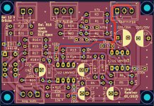
I have tested a few opamps but never really compared them by critical listening. The circuit itself will work with many unity-gain stable opamps. The component values, as discussed above, are optimized for the likes of LM4562 and NE5532. I do not have any pops when switching it on/off, so no relay is included in my implementation. Your PCB artwork looks ok but not great, and its performance is likely to be below the circuit's potential.
- Home
- Source & Line
- Analog Line Level
- My Balanced Line Receiver