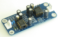
My balanced line receiver is a small PCB that adds a true balanced input to any amplifier, thus helping to avoid certain problems inherent in single ended (e.g. RCA) connections. Compared to integrated receivers such as THAT1200 series, the board offers an order of magnitude lower distortion (depending on the choice of opamps) and built-in DC removal, which makes a downstream DC blocking capacitor unnecessary.
This project is based on my prior series of volume control boards, which itself was based on Bruno Putzeys' a demo project that illustrated his article "The G-word, or how to get your audio off the Ground", first published in Linear Audio Vol.5. While the focus of those previous projects was volume control, I realized that the combination of a low-distortion balanced input and a ground sensing output is useful by itself, for example, in a monoblock or even a stereo power amplifier.
There was some interest in this receiver in the discussion of our Omicron headphone amplifier earlier this year, so in the coming days I will publish the schematic (post #6 below), measurements and other info on this little board that may be useful.
Last edited:
The primary raison d'être for this board is to eliminate grounding issues.
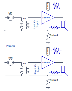
It all started some years ago with my build of Zen V4, where a single power supply was shared by two channels:
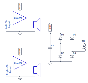
It worked really well on the bench, but when I connected both inputs to the preamp, I heard buzz from both speakers:
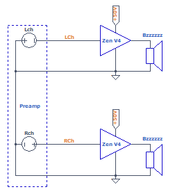
What was going on, of course, is that the two channels of the power amp and the preamp did not share the same "ground":
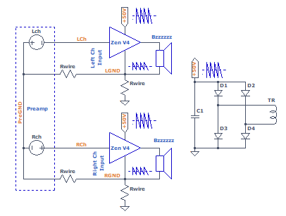
Although the connections were made with short and thick wires, the current drawn by each of the Class A power amp channels, and hence the AC component of the voltage drop on the wires, were large enough for the difference between LGND and RGND to be audible. I was lucky it was Class A - with a Class B amp, there would be no audible buzz, but the distortion caused by the same mechanism would still be there.
The problem stems from the fact that any audio amplifier with a single ended input has exactly one point that it considers the reference point from which the input signal is measured. In an inverting amplifier with a feedback loop (such as Zen V4), that point is the non-inverting input (in Zen V4, that's the source of the power MOSFET). In a non-inverting amplifier, that point is the bottom ("ground") end of the feedback divider:
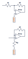
That is, each channel has its own "ground". Connect your input signal ground to any other point, and you will add noise and distortion to your signal.
There are several ways to cope with this grounding issue:
A balanced line receiver would be a lower distortion, cheaper option.
It all started some years ago with my build of Zen V4, where a single power supply was shared by two channels:
It worked really well on the bench, but when I connected both inputs to the preamp, I heard buzz from both speakers:
What was going on, of course, is that the two channels of the power amp and the preamp did not share the same "ground":
Although the connections were made with short and thick wires, the current drawn by each of the Class A power amp channels, and hence the AC component of the voltage drop on the wires, were large enough for the difference between LGND and RGND to be audible. I was lucky it was Class A - with a Class B amp, there would be no audible buzz, but the distortion caused by the same mechanism would still be there.
The problem stems from the fact that any audio amplifier with a single ended input has exactly one point that it considers the reference point from which the input signal is measured. In an inverting amplifier with a feedback loop (such as Zen V4), that point is the non-inverting input (in Zen V4, that's the source of the power MOSFET). In a non-inverting amplifier, that point is the bottom ("ground") end of the feedback divider:
That is, each channel has its own "ground". Connect your input signal ground to any other point, and you will add noise and distortion to your signal.
There are several ways to cope with this grounding issue:
- One is look the other way and be satisfied, for example, with no buzz or noise with one's ear against the speaker's grill, and call it quiet enough. However, even if you don't hear the buzz, it will create intermodulation products when you play some music, muddling the sound.
- Build a separate power supply for each power amp channel (a.k.a. "dual mono"), and a third for the preamp. This is by far the most popular approach, but also the bulkiest and the costliest. To me, having two power transformers in a 2x50W LM3886 based stereo amplifier is excessive.
- Use electronics to make sure each signal has its own correct reference - this is where balanced interconnect and ground sensing come handy. It is now a new approach - just have a look at e.g. Jensen Transformers application notes - but somehow this approach is rarely used in DIY amplifiers.
A balanced line receiver would be a lower distortion, cheaper option.
Last edited:
So a transformer breaks ground loops by making sure that each signal has its correct local reference a.k.a. "ground", even if these grounds are different:
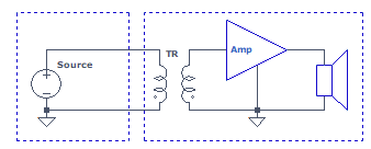
A transformer-less way of doing the same is well known:
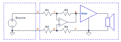
Here, feedback keeps points C and D at the same potential, and it is easy to see that the power amp's input voltage V(E,F)=-K×(V(A,B)), where K=R2/R1=R4/R3 is the equivalent of a transformer's turns ratio. As with a transformer, the difference between local grounds B and F doesn't affect the power amplifier's input.
The right end of R4 on the schematic above, marked F, is the equivalent of the grounded end of a transformer's secondary. It has to be connected to the local ground of the downstream amplifier and not anywhere else - this is the "ground sensing". Otherwise, noise and distortion will be added to the signal:

There are couple of practical limitations in this approach. First, the potential at points C and D must be within the common-mode input-voltage range of the opamp, which usually is well within its power supply rails. Because of that, local grounds B and F cannot be too far apart. This is easy to achieve if B and F are connected e.g. via a shared power supply within one chassis or by an interconnect shield if they are in two different boxes.
Second is that the attenuation of the difference between local grounds B and F (a.k.a. common mode rejection) depends on how close R2/R1 is to R4/R3. With 1% resistors, one can expect about 50dB (1/300) rejection, which seems to be enough for most practical purposes.
BTW one can buy differential line receivers with on-chip precision resistors:
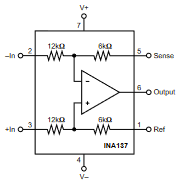
but these are more expensive yet inferior to modern opamps in distortion performance.
Common mode rejection can be affected by the output impedance of the signal source. For example, most sources have a resistor at the output for stability or other reasons:
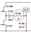
That output resistor is in series with R1, throwing the differential receiver off balance (that is, R2/(R1+Rsrc)≠R4/R3):
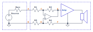
To reduce this effect, one can increase R1,R2,R3,R4 to make Rsrc small in comparison, but it is better to buffer each of the differential inputs:

Practically speaking, the buffers will need a path to ground for their input currents even if the source is capacitor coupled of disconnected, so a resistive network at the input is required:

Lastly, DC removal. Instead of a DC servo, my balanced line receiver uses an inverting low-pass filter (LPF) in parallel with R1 and R3 that makes the "turns ratio" zero at DC, just like with a real transformer. Here is a simplified schematic:
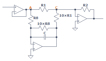
At DC, the gain of the LPF is ×(-10), and any DC current through R1 is cancelled by the opposite current flowing to point C from the LPF's output through the 10×R1 resistor. At AC, the gain of the LPF is small, so the cancellation effect is negligible.
A transformer-less way of doing the same is well known:
Here, feedback keeps points C and D at the same potential, and it is easy to see that the power amp's input voltage V(E,F)=-K×(V(A,B)), where K=R2/R1=R4/R3 is the equivalent of a transformer's turns ratio. As with a transformer, the difference between local grounds B and F doesn't affect the power amplifier's input.
The right end of R4 on the schematic above, marked F, is the equivalent of the grounded end of a transformer's secondary. It has to be connected to the local ground of the downstream amplifier and not anywhere else - this is the "ground sensing". Otherwise, noise and distortion will be added to the signal:
There are couple of practical limitations in this approach. First, the potential at points C and D must be within the common-mode input-voltage range of the opamp, which usually is well within its power supply rails. Because of that, local grounds B and F cannot be too far apart. This is easy to achieve if B and F are connected e.g. via a shared power supply within one chassis or by an interconnect shield if they are in two different boxes.
Second is that the attenuation of the difference between local grounds B and F (a.k.a. common mode rejection) depends on how close R2/R1 is to R4/R3. With 1% resistors, one can expect about 50dB (1/300) rejection, which seems to be enough for most practical purposes.
BTW one can buy differential line receivers with on-chip precision resistors:
but these are more expensive yet inferior to modern opamps in distortion performance.
Common mode rejection can be affected by the output impedance of the signal source. For example, most sources have a resistor at the output for stability or other reasons:
That output resistor is in series with R1, throwing the differential receiver off balance (that is, R2/(R1+Rsrc)≠R4/R3):
To reduce this effect, one can increase R1,R2,R3,R4 to make Rsrc small in comparison, but it is better to buffer each of the differential inputs:
Practically speaking, the buffers will need a path to ground for their input currents even if the source is capacitor coupled of disconnected, so a resistive network at the input is required:
Lastly, DC removal. Instead of a DC servo, my balanced line receiver uses an inverting low-pass filter (LPF) in parallel with R1 and R3 that makes the "turns ratio" zero at DC, just like with a real transformer. Here is a simplified schematic:
At DC, the gain of the LPF is ×(-10), and any DC current through R1 is cancelled by the opposite current flowing to point C from the LPF's output through the 10×R1 resistor. At AC, the gain of the LPF is small, so the cancellation effect is negligible.
Last edited:
Here is the full schematic:
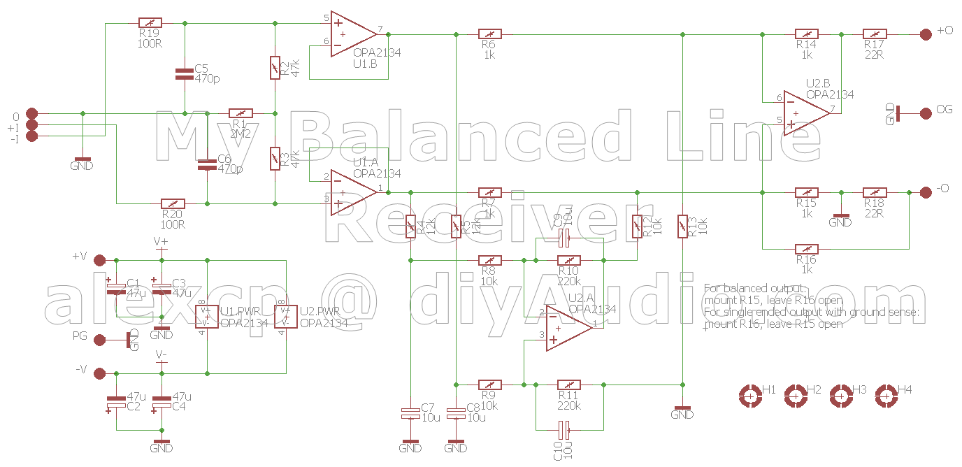
There are a few things that have not been mentioned so far in my previous posts:
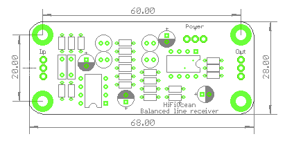
A photo of an assembled board, configured for ground sense output, is at the top of the first post in this thread.
There are a few things that have not been mentioned so far in my previous posts:
- There are EMI filters (C5R19 and C6R20) at both "hot" and "cold" inputs.
- The DC removal filter is 2nd order (with C7,C8) rather than 1st order.
- The output can be configured as ground sensing (see above) or as balanced (meaning hot and cold outputs with equal impedances, not two signals with opposite phase) - this can be useful if the downstream amplifier has a balanced input. This is done by mounting a 1k resistor as R15 for the balanced output or R16 for the single ended output with ground sense. Do not mount both R15 and R16 at the same time.
- Power supply for the opamps is shown, nothing unusual there.
A photo of an assembled board, configured for ground sense output, is at the top of the first post in this thread.
Last edited:
You're right, my front end is what Mr. Putzeys used in his demo project. In fact, this topic starts with a reference to his demo board, see the very first post. And yes, I surely did follow the guidelines from his article (and leveraged my own experience) in laying out this board, as I did earlier with my volume controls and a few other projects. The results show up in the board's measurements, which will follow.
Last edited:
Measurements, part 1. The board is fitted with 2x OPA2134 opamps.
Differential mode frequency response:
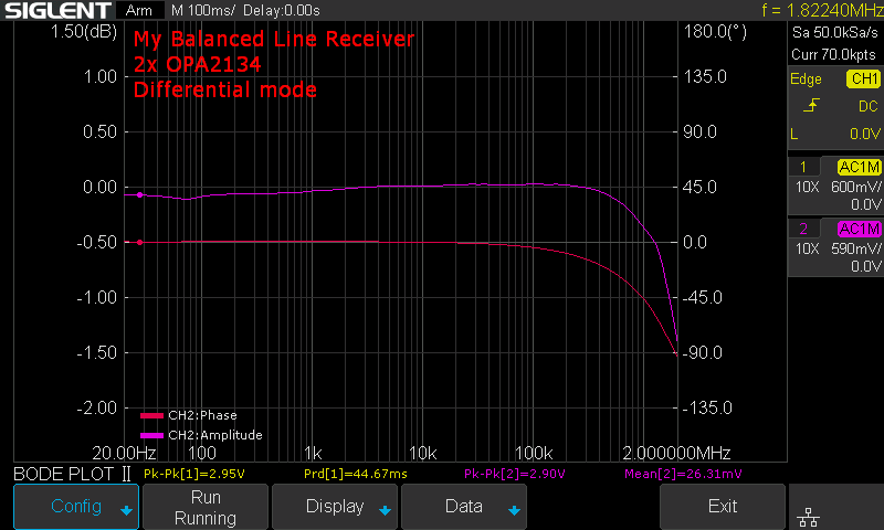
The receiver response is flat in the audio range, rolling off at higher frequencies. The roll off is defined by the source impedance (here. 50 ohm) and R19 R20 C5 C6 low pass filter (see the schematic in post #6 above).
Common mode rejection with matched hot and cold source impedances:
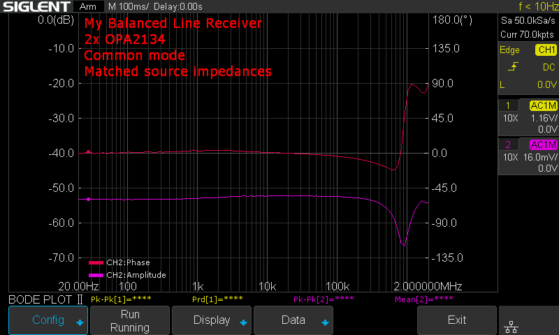
As mentioned in earlier posts, CMRR is limited by the 1% tolerance resistors used. Yet, it is better than 50dB (1/300) in a broad range of frequencies.
Common mode rejection with hot and cold source impedances mismatched by 10 ohm:
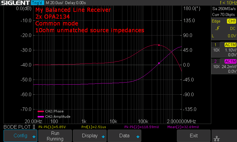
The CMRR at low frequencies in unaffected by the source impedance mismatch. However, the extra 10ohm impedance in the hot wire creates an LPF with C5 (see the schematic in post #6 above), which affect the CMRR above the audio range,
Common mode rejection with hot and cold source impedances mismatched by 600 ohm:

The CMRR at low frequencies in still unaffected by the source impedance mismatch. The HF effect seen with 10 ohm source impedance is amplified here, as the corner frequency of the parasitic LPF is now lower.
It is interesting to compare the above measurements to the datasheet of THAT1200 series balanced line receivers, which benefit from precision matched on-chip resistors, as well as the patented bootstrapping of the input network. THAT1200 has 5dB less CMRR at 20kHz than at 60Hz (flat in the case of my receiver) and about 20dB less CMRR with 600 ohm mismatched source impedance (which is about the same difference as I measured for my board).
More measurements to follow.
Differential mode frequency response:
The receiver response is flat in the audio range, rolling off at higher frequencies. The roll off is defined by the source impedance (here. 50 ohm) and R19 R20 C5 C6 low pass filter (see the schematic in post #6 above).
Common mode rejection with matched hot and cold source impedances:
As mentioned in earlier posts, CMRR is limited by the 1% tolerance resistors used. Yet, it is better than 50dB (1/300) in a broad range of frequencies.
Common mode rejection with hot and cold source impedances mismatched by 10 ohm:
The CMRR at low frequencies in unaffected by the source impedance mismatch. However, the extra 10ohm impedance in the hot wire creates an LPF with C5 (see the schematic in post #6 above), which affect the CMRR above the audio range,
Common mode rejection with hot and cold source impedances mismatched by 600 ohm:
The CMRR at low frequencies in still unaffected by the source impedance mismatch. The HF effect seen with 10 ohm source impedance is amplified here, as the corner frequency of the parasitic LPF is now lower.
It is interesting to compare the above measurements to the datasheet of THAT1200 series balanced line receivers, which benefit from precision matched on-chip resistors, as well as the patented bootstrapping of the input network. THAT1200 has 5dB less CMRR at 20kHz than at 60Hz (flat in the case of my receiver) and about 20dB less CMRR with 600 ohm mismatched source impedance (which is about the same difference as I measured for my board).
More measurements to follow.
Last edited:
Nice results. These confirm the benefits of the balanced line stage as implemented here.
In the original Putzeys version of the stage, LM4562 bjt op-amps were used while you have opted for OPA2134 fet op-amps. My understanding is that the LM4562 is particularly suited to low source impedance circuits while the OPA2134 (like most fet devices) is more suited to higher source impedances, especially regarding noise performance. To aid in our understanding of the overall circuit, can you give an outline of your design choices here?
In the original Putzeys version of the stage, LM4562 bjt op-amps were used while you have opted for OPA2134 fet op-amps. My understanding is that the LM4562 is particularly suited to low source impedance circuits while the OPA2134 (like most fet devices) is more suited to higher source impedances, especially regarding noise performance. To aid in our understanding of the overall circuit, can you give an outline of your design choices here?
Here, the OPA2134 is not so much a design choice as it is an example. The circuit performs well with a broad variety of dual opamps with both FET and BJT inputs, even with good old TL072 and NE5532, and the through hole construction of the board with socketed opamps encourages opamp rolling.
On the noise, you are correct that BJT input opamps are somewhat quieter than FET input in low impedance circuits. (The former tend to have lower voltage noise, and their higher current noise doesn't matter so much with low impedances.) In this particular case, however, the difference is rather small (a few dB) and probably doesn't matter, as in either case the total RMS noise level over 20-20kHz is low single microvolts.
If you refer to Figure 25 in Putzey's original article:
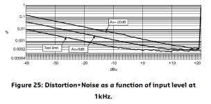
you will see those microvolts with the LM4562. Say at Av=1 (that is, the volume control at 12 o'clock) and -10dBu (about 250mV RMS), the THD+N is just above 0.001%, or 2.5μV. With the OPA2134, my simulation shows just below 3.2μV.
On the noise, you are correct that BJT input opamps are somewhat quieter than FET input in low impedance circuits. (The former tend to have lower voltage noise, and their higher current noise doesn't matter so much with low impedances.) In this particular case, however, the difference is rather small (a few dB) and probably doesn't matter, as in either case the total RMS noise level over 20-20kHz is low single microvolts.
If you refer to Figure 25 in Putzey's original article:

you will see those microvolts with the LM4562. Say at Av=1 (that is, the volume control at 12 o'clock) and -10dBu (about 250mV RMS), the THD+N is just above 0.001%, or 2.5μV. With the OPA2134, my simulation shows just below 3.2μV.
If you take the ratio of voltage noise to current noise you get the optimum source impedance to match the opamp and get best noise factor out of it (keeping input signal power constant).
In the olden days the lack of range of active devices encouraged the ploy of using a transformer(*) to match the source impedance to the input stage's best noise impedance - these days there's quite a wide range available from AD797 at the low impedance end to JFET and CMOS opamps at the high end. The various vaguaries of such wound components can generally be avoided as a consequence (although they can be simulated in a DAW if you really want!)
Its amazing how technology progresses - for instance CMOS input opamps can now be made to rival JFET types for noise performance, certainly big strides have been made with CMOS analog performance.
Oddly the NE5534A remains one of the highest noise-impedance bipolar opamps available, few other bipolars can match it at the 10k to 30k impedance realm (common in active circuitry like filters/EQ etc). The LM4562 is not great noise-wise up at 20k ohms, its best performance is in the 1k to 2k realm which vindicates your choice of resistor values. In fact the AD797, LM4562 and NE5534A are all similar performers in that impedance range I reckon from the data...
(*) and this provides balanced inputs and/or outputs for free!
Thank you @Mark Tillotson for the incredibly insightful post!
The next part of the measurements is the ground sense function.
The measurement is taken from the point of view of the downstream amplifier that gets its input signal from the balanced line receiver's output. The balanced line receiver's input is shorted, and its ground is wiggled w.r.t. the downstream amplifier's ground. The chart shows the proportion of that wiggle that the downstream amplifiers sees at its input.
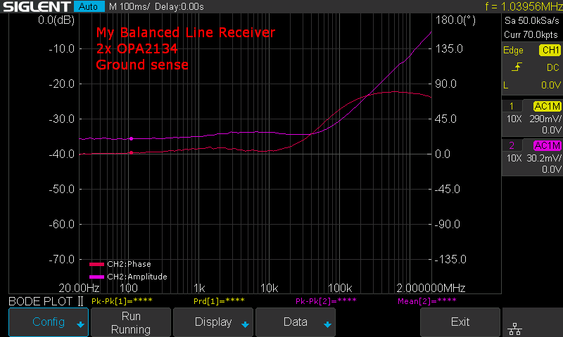
Here we see the ground wiggle is suppressed by some 35dB (1/50) in the audio range. As was the case with CMRR above, the suppression is limited by the tolerance of the 1k resistors around U2.B (see the schematic above).
The next part of the measurements is the ground sense function.
The measurement is taken from the point of view of the downstream amplifier that gets its input signal from the balanced line receiver's output. The balanced line receiver's input is shorted, and its ground is wiggled w.r.t. the downstream amplifier's ground. The chart shows the proportion of that wiggle that the downstream amplifiers sees at its input.
Here we see the ground wiggle is suppressed by some 35dB (1/50) in the audio range. As was the case with CMRR above, the suppression is limited by the tolerance of the 1k resistors around U2.B (see the schematic above).
By the way I notice there's no input protection - I'm thinking of the scenario where its powered down when there's a large incoming signal - the input opamps may not like that as there's only 100 ohms between them and connector, adding some protection diodes to those opamp inputs to the rails might be worth having (1N4148's are probably OK, though Schottky might be more thorough protection).
Opamps are usually well protected when powered up, so long as inputs stay within supply range, but powered down may be vulnerable - I suspect this varies considerably between devices Ive rarely seen it mentioned in datasheets.
Opamps are usually well protected when powered up, so long as inputs stay within supply range, but powered down may be vulnerable - I suspect this varies considerably between devices Ive rarely seen it mentioned in datasheets.
Here is a distortion comparison between SSM2141, THAT1206 and the above balanced line receiver with 2x OPA2134 and 2x LM4562. In all graphs, the balanced line receiver drives a 2kOhm load to 6Vpp (2.1V RMS) at 1kHz. 2.1V RMS corresponds to 0dB on the graphs, but the fundamental is suppressed to eliminate the measurement rig's own distortion. Only the hot input of each receiver is driven; the cold is grounded. For THAT1206, the input level is 4.2V RMS, as its gain is -6dB. For the rest the gain is unity, so the input signal is 2.1V RMS.
SSM 2141, THD=0.000 5%:
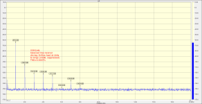
THAT1206, THD=0.000 3%:
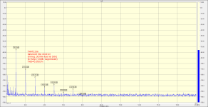
This balanced line receiver with OPA2134, THD=0.000 1%:
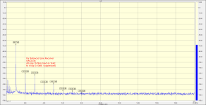
This balanced line receiver with LM4562, THD=0.000 02%:
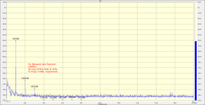
SSM 2141, THD=0.000 5%:

THAT1206, THD=0.000 3%:

This balanced line receiver with OPA2134, THD=0.000 1%:

This balanced line receiver with LM4562, THD=0.000 02%:

I'm interested, for one.If there is interest, perhaps we can do a group buy for the boards?
- Home
- Source & Line
- Analog Line Level
- My Balanced Line Receiver