I understand.
I will leave it to you to substitute the .models you already have at hand in place of the MJL's 3281/1302. You can use MJE15032/15033 as substitutes for MJE340/350 in my simulation and try this out with Miller compensation.
I have seen the odd instance where the closed loop gain is high enough allows the use of step feedback arrangements from the Vas collector to the inverting input - which seems to offer some flexibility with where the stability margins are set.
The downside to this is this approach is likely to give rise to a peak in the Tian plot with increasing capacitor values and stopper resistors are needed for dampening effect.
Although that said these should serve a useful safety purpose if there is an output stage failure.
I have revised the previous simulation to show how this works around the added components R38 and C8. The original Miller capacitor is in place so you can compare by removing traces to switch whichever one you want to look at.
The layout for a circuit will require more circuit board space for the output stage - it may pay to aim for higher stability margins to avoid risks of the layout.
Again this is mostly off the cuff since I was planning a holiday and we have finally gotten away from home this morning.
I have not built an amplifier of these proportions maybe others who have done so could comment from their experiences.
Attachments
Last edited:
I will take Mooly's advice and set the targets for this project.
The Objectives:
a) Use an existing driver and power stage (taken from Wharfedale S1500)
b) Design/find a SUITABLE VAS and input differential stage
c) The input differential transistors must be isolated from the high voltage using a suitable method. I used a cascode with high voltage transistors.
d) Use the SAME chassis and power supply.
e) Use the existing DC voltages of +85V, 0V (ground), -85V
The Consequences:
i) High voltage VAS transistors are a requirement that cannot be workedaround.
The MINIMUM Vceo voltage is 85x2 + safety_margin. The EXISTING driver stage uses MJE15032 and MJE15033 which are RATED AT Vceo = 350V.
Attachments
Last edited:
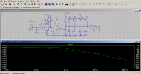
From now on I will concentrate on this circuit. See the attachment in which the Miller capacitor and feedback loop are disconnected.
With a signal voltage of 1000mV, the open loop gain is a staggering 96dB. However, with a signal of 1mV the open loop gain drops considerably to a mere 36dB.
With a signal voltage of 1000mV, the open loop gain is a staggering 96dB. However, with a signal of 1mV the open loop gain drops considerably to a mere 36dB.
Attachments
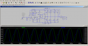
Ib(driver_transistor) and Vout under open loop conditions.
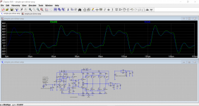
The attachment show the output waveform under open loop conditions. There is far less ringing of base current of the driver transistor. The distortion with this high output level is around 10%. The simulated signal frequency is 16kHz.
It is interesting to investigate why under open loop conditions the driver's base rings considerably less than when the loop is closed.
PS: [More Testing]
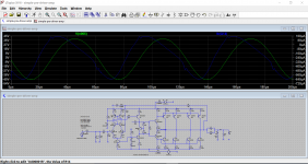
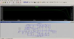
With the feedback loop closed and the Miller capacitor connected. Up to 9.35V peak output, there is practically NO ringing of the driver base current. The ringing appears as a kink that is just noticeable.
The attachment show the output waveform under open loop conditions. There is far less ringing of base current of the driver transistor. The distortion with this high output level is around 10%. The simulated signal frequency is 16kHz.
It is interesting to investigate why under open loop conditions the driver's base rings considerably less than when the loop is closed.
PS: [More Testing]
With the feedback loop closed and the Miller capacitor connected. Up to 9.35V peak output, there is practically NO ringing of the driver base current. The ringing appears as a kink that is just noticeable.
Attachments
Last edited:
You can achieve similar results by making the feedback return cap very large (try '1' which is 1F, don't enter 1F though which is 1 Femto in LTspice). Doing it this way preserves the correct DC conditions. Short out the feedback return resistor.
This is with 10mv applied to the input.
This is with 10mv applied to the input.
Attachments
Thanks for the trick of eliminating feedback without having to find a suitable resistance to pull the output to zero volts under no signal conditions.
Using an emitter resistance of 56 Ohms for differential pair pulls the open loop gain down to:
At 10Hz: ~300 times
At 16kHz: ~150 times.
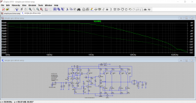
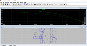
I don't know what open loop gain is best suited for maximal stability. With the above open loop gain, the AC Analysis is as attached.
Using an emitter resistance of 56 Ohms for differential pair pulls the open loop gain down to:
At 10Hz: ~300 times
At 16kHz: ~150 times.
I don't know what open loop gain is best suited for maximal stability. With the above open loop gain, the AC Analysis is as attached.
Attachments
The peak in your response is because you are measuring after the output inductor which means the inductor reacts with the load capacitance. Try measuring before the inductor.
I think conventional wisdom suggests you should really be aiming for a high open loop gain. My own amp, which is very uncomplicated achieves high OLG using just a single ended input stage.
I think conventional wisdom suggests you should really be aiming for a high open loop gain. My own amp, which is very uncomplicated achieves high OLG using just a single ended input stage.
Attachments
With an emitter resistance of 12 Ohms the open loop gain is:
At 10Hz, 98dB
At 16kHz, 66dB
Without an emitter resistance the open loop gain maximum is 102dB.
At 10Hz, 98dB
At 16kHz, 66dB
Without an emitter resistance the open loop gain maximum is 102dB.
Last edited:
With differential pair emitter resistors of 12 Ohms and with the output filters disconnected, this is the square wave test with a slew rate of 15 million volt/sec.
Attachments

Last edited:
Making the load slightly capacitive by connecting a 1uF capacitor in parallel, oscillation occurs quite vigorously.That looks pretty good actually. Nicely shaped and no suspicion of oscillation.
Twin wires have capacitance which cannot be eliminated. With the inductor the oscillations are greatly reduced but the overall shape of the square wave is not as neat as that with a purely resistive load.
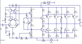
Looking at this design, IME, you guys have a potentially thermally unstable OP stage.
If we take the MJE340/350 drivers, for an increase of 1mA quiescent, EACH OP device will have an increase of 30mA (x 4 = total 120mA).
Since the VBE is a BC337, if it is a TO92 case you will have some issues achieving the required thermal coupling as the whole OP stage, being VBE, drivers and OP devices will need to be VERY well thermally coupled.
If thermal stability ends up being an issue, try the following:
- Use small flat pack BJT for the VBE bias transistor and clamp it close to OP devices on the heatsink.
- IME, you can tweak the thermal 'feedback' by the current rating (geometry) and early voltage of this transistor. For example if the OP stage tends towards thermal runaway, try a VBE BJT of higher current rating and observe it's behavior.
- Insert some small value resistors, (say 0.05 ohm) resistor in series with R24 / R27 which becomes OP device collector connection point. This will provide current run-away feedback.
WRT actual amp stability, my, and many other peoples experience is that CFP OP stages love to oscillate - in real life as opposed to in simulators.
If this occurs, try some small value base stopper resistors on the OP BJT's.
Edit: schem added below for ref
cheers
T
Attachments
Last edited:
Thanks for the warning. In my native language, not english, there is a saying which goes something like this: "Prewarned is half armed". Maybe, you don't know, that this power stage, is the power stage used by Wharfedale S1500 amplifier. This project is to bring that amplifier to life but with major changes.Looking at this design, IME, you guys have a potentially thermally unstable OP stage.
I am taking your advice/warning to try mitigating thermal changes in the bias currents. At constant current, the voltage across a diode decreases by 2mV/K. A 10K temperature increase corresponds to a -20mV change. A diode can easily be used instead of a resistor in the amplified diode without drastic circuit changes.
P.S. I changed the amplified diode transistor to BD136 which can be mounted on heatsink. Vbe will change by -2mV/K, which means in our case, an overall change of: (470 + 415)*(-2x10^-3)/470 volts/K = -3.766mV/K
For a temperature increase of 30K, this will result in a bias voltage change of: -3.766x10^-3*30 = -113mV/K
From this calculation it seems the voltage drop due to thermal increase is too big. This is an opinion, so constructive comments are very helpful.
In agreement to what you warned me against, simulating a global circuit temperature of 60 degrees Celcius, the quiescent bias current per pair increased to 300mA. Such a current is destructive if not properly controlled. The output transistors are particularly sensitive to thermal runaway: this is clearly stated in the manufacturer's datasheets.
So, the next aim is to stabilise the circuit againt thermal runaway in the output stage. Simulating for a global temperature of 20C and 60C, the bias voltage across the amplified diode is:
@ 20C Vbias = 1414.119mV
@ 60C Vbias = 1275.409mV
This voltage drop with a hotter temperature is NOT enough as the quiescent current increased by a very large factor.
Again, thanks a lot.
===
Douglas Self's book on page 415 has a Vbe multiplier with increased tempco that I can use in this circuit. Transistors and heat do not go well together.
The following list shows Vbias Vs Temperature. The resultant requirement for quiescent current constancy is -6.8mV/K. Vbias must drop by -6.8mV/K.
This is the data:
20C, 1436.28mV, 11.267mA
30C, 1368.87mV, 11.335mA
40C, 1301.78mV, 11.975mA
50C, 1233.19mV, 11.956mA
60C, 1164.04mV, 11.986mA
70C, 1093.39mV, 11.548mA
Thank goodness the relationship is linear.
Vbias = 1436 + (20 - T)*6.8
Vbias = 1572 - 6.8T
WRT actual amp stability, my, and many other peoples experience is that CFP OP stages love to oscillate - in real life as opposed to in simulators. If this occurs, try some small value base stopper resistors on the OP BJT's.
Edit: schem added below for ref
cheers
T
The non-linear emitter diode resistance is in the path from the supply rail to the base which is your control point. In this circuit the output emitters connect to the supply rail which is not beyond suspicion for cleanliness as might be the case with a line like the speaker feed where negative feedback would clean some of that up.
I put small resistors in series with the base so most of the voltager drop from current entry draw point to exit is across the resistor and not the non-linear diode resistance. I did this in the simulation attached to post 221 where these resistors also help to split the feed. In all these simulations the output transistors are matched sets - this does not happen in real life.
Fast forward to the latest rendition of the circuit - these are redundant. The phase margin may be -60 degrees but the gain margin is only -6 dB under the ideal conditions of the simulation. As I see it there are risks needing to be mitgated here. It would not be a bad thing to run the supply for the small signal stage from a separately rectified power supply source.
Problem: Drivers heating up conducting more and more current with the same bias voltage.
Attempting Solutions: Use a temperature dependent resistor or the junctions of a transistor or a diode pusposely mounted in good thermal contact on top of a driver on the main heatsink.
Attempting Solutions: Use a temperature dependent resistor or the junctions of a transistor or a diode pusposely mounted in good thermal contact on top of a driver on the main heatsink.
One characteristic of the stability of this circuit is when the standing current through each output transistor is low the stability will be high. Since the driver transistors fill the crossover region the outputs should be allowed to work at low standing currents. You can see this in the simulation attached to post 221 by changing the value of R4 from 990 to 960. This will have the effect of changing the stability margins. The gain margin will decrease by near enough to 10 dB albeit the phase margin will increase by 6 degrees. This came about by the rather insignificant act of increasing the per output transistor standing current from 2 m.A. to 6 m.A.
In a way the output transistors might be regarded in the sense of dumping current. It seems this has some rather awkward effects on phase - imagine the effect on gain and phase margin when the output currents are high. If the stability gain margin is only 6dB in your latest circuit you might like to monitor your changes more closely. Had you adapted my Tian probe simulation to changes you made you would have seen this. R8 and R18 and 19 in my simulation are not thoughtless additions to the original circuit with regard to temperature. In that regard neither is C6 regarding stability.
In a way the output transistors might be regarded in the sense of dumping current. It seems this has some rather awkward effects on phase - imagine the effect on gain and phase margin when the output currents are high. If the stability gain margin is only 6dB in your latest circuit you might like to monitor your changes more closely. Had you adapted my Tian probe simulation to changes you made you would have seen this. R8 and R18 and 19 in my simulation are not thoughtless additions to the original circuit with regard to temperature. In that regard neither is C6 regarding stability.
Last edited:
I am simulating high temperatures for the power stage's drivers and amplified diode. Till now, I am getting a 'time bomb' as increasing the temperature is having a disastrous effect on the power stage's quiescent current.
[Iq is power stage's quiescent current per pair]
At 27C, Iq = 10.7mA
At 35C, Iq = 27.5mA
At 45C, Iq = 65.8mA
At 55C, Iq = 119.3mA
At 65C, Iq = 182.1mA
At 85C, Iq = 322.1mA
At 95C, Iq = 395.9mA
At 105C, Iq = 471mA
At 115C, Iq = 547mA
P.S. Thanks to Douglas Self, now after using a temperature compensated amplified diode, at 27C the quiescent current is 9.6mA which increases to 25.2mA at 65C. This looks very good. A little more fine tuning and the circuit will have temperature compensation.
After more compensation fine tuning, the quiescent current per pair is as follows:
At 27C, 8.6mA
At 75C, 22.2mA
At 100C, 36.2mA
At 120C, 53.3mA
The 100C and 120C are given only for reference. Even at 75C, an amplifier would be too hot to serve a long lifetime.
Attachments
Reading Douglas Self, it seems, he does not like CFP output stages like this. Simulating for high temperatures of the drivers, amplified diode transistor and output transistors, I am getting the impression that this output stage is not optimal both for quiescent current stability and freedom from self oscillation. This is making me think about changing the power stage topology to that of a real emitter follower as found on most power amplifiers. Also, simulating for the latter output stage, I found they have a far better quiescent current balance. For most quiescent currents, the difference between the PNP and NPN transistors was 0.1mA.
The fact that a practically new amplifier failed, is telling me that there were questionable design decisions with this design. Yes, an emitter follower power stage forces one to use insulators for the power transistors, but that, should never be an issue where high power is involved. High power requires stability to be taken very seriously. This is why I am so hesitant to start making the PCB. First, it must behave well on simulations, then, do other evaluations, and finally, make the PCB and actual circuit.
Thanks to mjona I will include 2.2 Ohm base resistors to improve stability.
Last edited:
Some Explanations
A CFP has better temperature management than an emitter follower arrangement however the output structure of this circuit is not a CFP as there is a missing feedback resistor between the output transistors and the drivers.
In the present circuit if the driver transistors are allowed to heat up these will draw more current through the collector load resistors increasing the voltage drop across these. Accordingly the voltage at the base of the outputs will be made lower.
The difference between the output base voltages will then increase and more current will be drawn. You would not put the driver transistors on the same heat-sink as the outputs - these need an adequate separate heat-sink
The 220R stopper resistors in the driver transistor bases will put some limit on the base current and mitigate some of the risk.
The 27R resistor in the vbe circuit restricts current through all three transistor connections and this amended structure resembles a common emitter amplifier making it more sensitive to temperature.
The place for the sense transistor is on the same heat-sink as the driver transistors.
It appears that the output transistors can run with the bases a fraction below the voltage turn on threshold as the drivers will bridge the crossover gap between the separate output halves. You could aim the bias setting such that as the driver transistors warm up the standing current in the output transistors crosses the conduction threshold.
I perceive there are significant differences in phase in the output stages of this circuit.
In my simulations such defeated attempts to compensate by the usual Miller capacitor. The only way to correct for these was to derive some feedback from the Vas collector to short circuit these high frequency effects. The additional capacitor C6 was included for that purpose.
- Home
- Amplifiers
- Solid State
- My attempts at a design of a 3 stage amplifier