Well spotted on Q9 🙂
I must have been playing around with something ages ago and saved the file like that. A 2N5551C and 372 ohms for the bias preset will give the correct 100ma Iq
I must have been playing around with something ages ago and saved the file like that. A 2N5551C and 372 ohms for the bias preset will give the correct 100ma Iq
It doesn't seem to make any difference to the ringing once the bias current is set correctly. Generic NPN model and 460 ohm looks similar to a 2N5551C and 372 ohm. Both give around 100ma Iq.
First of all, thanks for taking interest in this thread. Yes, I am interested in what you have done to get rid of ringing. Please, post the .asc file. This thread is a long journey to design an amplifier, it is like an adventure and a learning experience.
P.S.
I am repeatedly finding that the output stage is the source for ringing. Increasing the quiescent current of the output does away with all ringing, but this solution, is very unattractive energy-wise. I also found increasing the VAS's current source's current attenuates the ringing. However, changing the VAS's quiescent current does not prevent all ringing.
The pivot question is how much quiescent current does a 2SC5200 transistor usually needs in a Class AB configuration?
Last edited:
Bias current depends on topology and component values, however following Doug Selfs extensive work on this the optimum bias would be around 12ma per pair.
At this point, I will content myself with Thomas A. Edison's quote: "Many of life's failures are people who did not realize how close they were to success when they gave up."
I know, I might be close to what I want, but I am yet not there. A simulation is like calculus, but instead of being based on Algebra, it is based on numerical processing using a computer. In a simulation, my logic tells me, only DC conditions exist, just like in calculus, where an increment is infinitesimal, implying pseudo-static conditions. A capacitor becomes a battery with series/parallel resistors, an inductor becomes a battery whose voltage is equal to the rate of change of current flowing through it, etc.
Simulations are humanity's gift from computers.
Fortunately you have the advantage of being able to examine and simulate other peoples designs on this site and extend your knowledge that way.
You can also learn from manufactured designs by looking at service manuals.
I think it would be better to do this project in steps - the first of which would be to build and test a lower power prototype version and get that to work.
This will take out the complexity of driving a multiple output transistor stage. You can get a nasty shock from 87 volt supply rails with other possible safety issues while setting up or fault finding.
A further thought on a lower power output prototype is that some features of Self's Invariant Load Power Amplifier could be of interest. I have a simulation that I downloaded a while ago among my .asc files.
The prototype was built the first thing before I joined this forum and uses the same output stage. It requires some tweaking to balance its input differential pair. As it is, it has a narrow bandwidth up to about 4kHz after which the amplification factor drops drastically. The distortion is about 4%-5% as high frequency harmonics cannot be amplified properly. I simulated the circuit and succeeded to reduce the distortion to about 0.1% by changing the Miller capacitor which entended the frequency range to cover the entire audio range. The input differential pair quiescent currents were not balanced; changing two resistors rectified this issue.
The advice of avoiding using a voltage of +/-85V at first is a good advice. The circuit will first be tested using a voltage of around 15V per rail, and when the time comes to connect to the high voltages, a high power incandescent lamp will be connected in series of the power transformer. In the event of a fault, the rectified DC voltages will drop helplessly as current will be heavily limited. If the circuit works, the voltages will not drop to low levels.
On a different note:
I noticed that most audio amplifiers use PNP transistors for the input differential pair. What is the reason for this? Is it true PNP transistors as a differential pair result in a lower white noise? I have a version of the amplifier with a PNP transistor differential pair input but it suffers from some ringing albeit heavily reduced.
PNP could offer lower noise I believe (historically) but that may be more applicable to preamp circuitry.
I've always thought one reason was that using PNP for the front end usually allows for an NPN VAS stage following, and usually high voltage high gain NPN's are much more readily available and better performing.
I've always thought one reason was that using PNP for the front end usually allows for an NPN VAS stage following, and usually high voltage high gain NPN's are much more readily available and better performing.
The advice of avoiding using a voltage of +/-85V at first is a good advice. The circuit will first be tested using a voltage of around 15V per rail, and when the time comes to connect to the high voltages, a high power incandescent lamp will be connected in series of the power transformer. In the event of a fault, the rectified DC voltages will drop helplessly as current will be heavily limited. If the circuit works, the voltages will not drop to low levels.
You could make a decent prototype using rail voltages of about 35-40 volts. I have downloaded your .asc file and for the sake of curiosity and interest I will look further into this with that in mind.
50 Watt Version
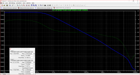
I am quite surprised how well this circuit simulates and am attaching some preliminary views of THD and Tian probe results. The results for THD are at 28.5 volts peak output. I did the Tian probe test before this at 27.5 Volts peak but there is no difference with the re-run I did after the screen shot was taken.
I changed a number of transistor types and reduced the supply rails to 40 volts.
The output devices are MJL21193 and MJL21194. I made the drivers BD139 and BD140.
The collector and emitter currents are roughly equal in these. The MJL's standing current is about 10 m.A. paying heed to the mention of the findings of Self.
There are a few other points to make about the circuit and I am gathering some thoughts for later. I will post my .asc files in due course.
Attachments
More on a 50 Watt version
I see in post 11 a warning about the level of gain that would arise from using a cascode LTP in combination with current mirrors. For the version I have tested that is about 100 dB of loop gain at 1Hz.
The feedback factor seems to have been mitigated by using a relatively large closed loop gain of 51 which would work against interests of low THD at 20kHz.
I thought a better approach is possible where the closed loop gain was a little less - about 19.3 with the divider ratios I decided to use in my simulation.
The input impedance of this circuit is low and it would be better to buffer inputs with a line amplifier with a suitable level of gain.
I have made changes to nearly all of the semi-conductor line up using mostly Bob Cordell's .models. In other instances I have used ones from the LTSpice library because these are better suited to use at higher voltages.
The parts in my selection should be readily available at relatively low cost and I have considered where these are best deployed within the circuit.
I have looked at some high voltage parts like 2N5551 and 2N5401 which may work in some positions which could be the case for an uprated power version.
The dc offset remains an issue with this version and I had to reduce the input resistor R12 down to -15 m.V. There were two small alterations to the simulation I made which improved the THD at 20 kHz.
I have looked for other ways to get the dc offset a bit lower - this involves adding 68R resistors to the current mirror transistors which increases the THD a fraction. I have a separate simulation for that in reserve.
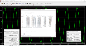
For the Tian probe the expression -1/(1-1/(2*(I(Vi)@1*V(x)@2-V(x)@1*I(Vi)@2)+V(x)@1+I(Vi)@2)) is shown in blue on the file.
Copy this and run the simulation. When the .raw file appears right click on the title in green vin and when a drop down box appears showing this delete it and paste in the expression copied. Then select the option to use two cursors drag cursor 1 to coincide with 0 dB as close as possible. The keyboard side arrows allow more accurate placement in fine steps. Then do likewise with cursor 2 to set this at -180 degrees.
The gain and phase margins will appear in the box at the bottom of the screen.
This simulation can be used to check stability effects arising from changes if anyone is interested in experimenting. A couple of things to note is the presence of a 27R resistor in the Vbe circuit which is contrary to the way Self does this but in accord with Julian Vereker and John Linsley-Hood. The compensation scheme is around the voltage gain stages - I tried Miller compensation early in the piece. The feedback network is low impedance by choice to allow a low value of compensation capacitor - value almost nothing.
I see in post 11 a warning about the level of gain that would arise from using a cascode LTP in combination with current mirrors. For the version I have tested that is about 100 dB of loop gain at 1Hz.
The feedback factor seems to have been mitigated by using a relatively large closed loop gain of 51 which would work against interests of low THD at 20kHz.
I thought a better approach is possible where the closed loop gain was a little less - about 19.3 with the divider ratios I decided to use in my simulation.
The input impedance of this circuit is low and it would be better to buffer inputs with a line amplifier with a suitable level of gain.
I have made changes to nearly all of the semi-conductor line up using mostly Bob Cordell's .models. In other instances I have used ones from the LTSpice library because these are better suited to use at higher voltages.
The parts in my selection should be readily available at relatively low cost and I have considered where these are best deployed within the circuit.
I have looked at some high voltage parts like 2N5551 and 2N5401 which may work in some positions which could be the case for an uprated power version.
The dc offset remains an issue with this version and I had to reduce the input resistor R12 down to -15 m.V. There were two small alterations to the simulation I made which improved the THD at 20 kHz.
I have looked for other ways to get the dc offset a bit lower - this involves adding 68R resistors to the current mirror transistors which increases the THD a fraction. I have a separate simulation for that in reserve.
For the Tian probe the expression -1/(1-1/(2*(I(Vi)@1*V(x)@2-V(x)@1*I(Vi)@2)+V(x)@1+I(Vi)@2)) is shown in blue on the file.
Copy this and run the simulation. When the .raw file appears right click on the title in green vin and when a drop down box appears showing this delete it and paste in the expression copied. Then select the option to use two cursors drag cursor 1 to coincide with 0 dB as close as possible. The keyboard side arrows allow more accurate placement in fine steps. Then do likewise with cursor 2 to set this at -180 degrees.
The gain and phase margins will appear in the box at the bottom of the screen.
This simulation can be used to check stability effects arising from changes if anyone is interested in experimenting. A couple of things to note is the presence of a 27R resistor in the Vbe circuit which is contrary to the way Self does this but in accord with Julian Vereker and John Linsley-Hood. The compensation scheme is around the voltage gain stages - I tried Miller compensation early in the piece. The feedback network is low impedance by choice to allow a low value of compensation capacitor - value almost nothing.
Attachments
Last edited:
In order to clean the amplifier driver stages of parasitic ascillations, I am trying to investigate the transconductance of the input stage, the voltage gain of the VAS and the slew rate.
Using I(difference_out)/V(in) I got a 920000A/V. This is shockingly huge!
The VAS:
a)With the output loaded.
The VAS's Voltage/I(difference_out) is 661V/A. I(difference_out) feeds the base of VAS's transistor.
b) Without the output load:
VAS's Voltage/I(difference_out) is 800V/A.
My *inexpert* observation is that the VAS's gain is low whereas the differential input transconductance is huge.
Please, note this is now an amplifier using a PNP input stage. It is based on the latest circuit I posted.
Attachments
Compensation make BIG different: https://www.diyaudio.com/forums/solid-state/317335-oitpc-output-inclusive-tpc-tmc-9.html#post5564178
The purpose of this project is to re-incarnate a large PA amplifier that failed. The make is Wharfedale and model is S1500 which has a +/- 85V DC power supply. My aim is to keep the power and driver stages intact and change the pre-driver circuitry together with the grounding scheme. I want to have the 0V as the ground and to have the power output between the 0V and the hot terminal of the output. In the original design, the hot terminal of the output was grounded with the result of op-amps having their non-inverting and inverting inputs interchanged. I do not want the hot output interfering with the ground, as this may cause unwanted parasitic paths that may destroy the input of any connected equipment. The amplifier's input would also be at risk with such a weird earthing scheme.
The drivers are MJE15033 and MJE15032. These are high voltage transistors, 350V. The only hurdle that is preventing me from building the circuit are parasitic oscillations in the latter two transistors, VAS's transistor and input. For the life of me, I haven't managed to understand the mechanism that is causing these weird oscillations.
The drivers are MJE15033 and MJE15032. These are high voltage transistors, 350V. The only hurdle that is preventing me from building the circuit are parasitic oscillations in the latter two transistors, VAS's transistor and input. For the life of me, I haven't managed to understand the mechanism that is causing these weird oscillations.
You might get some informative replies if you pose this question of the driver and VAS oscillation over in the BT thread.
John Curl's Blowtorch preamplifier part III
John Curl's Blowtorch preamplifier part III
The only reply I got was "Wrong thread" but nevertheless I thank you for taking some of your time to reply to my thread.You might get some informative replies if you pose this question of the driver and VAS oscillation over in the BT thread.
John Curl's Blowtorch preamplifier part III
Naturally, I am investigating the source of the ringing in the driver stage. My results show that it is the power stage that is causing a sort of weird feedback. I came to that conclusion by simulating a signal source of 60V with a frequency of 16kHz directly driving the driver stage. I also used a bias for the driver transistors to operate in Class AB. The result is clear: with a completely different pre-driver circuit the driver transistors still oscillate. To further test my conclusion, I used the latest circuit I posted here, but with transistors having their base disconnected with their emitters connected to the bases of the driver transistors, and their collectors connected to the points on the VAS, where the driver transistors should normally be driven. With this latter arrangement, it came crystal clear, surges of current are drawn from the VAS.
The logical solution is to devise a post-VAS pre-driver interfacing circuit that presents a very high impedance to surges of current but allows other currents to flow normally. The converse is done to drive MOSFETS of switching power supplies.
The purpose of this project is to re-incarnate a large PA amplifier that failed. The make is Wharfedale and model is S1500 which has a +/- 85V DC power supply. My aim is to keep the power and driver stages intact and change the pre-driver circuitry together with the grounding scheme.
The drivers are MJE15033 and MJE15032. These are high voltage transistors, 350V. The only hurdle that is preventing me from building the circuit are parasitic oscillations in the latter two transistors, VAS's transistor and input. For the life of me, I haven't managed to understand the mechanism that is causing these weird oscillations.
There are a number of things you need to consider. Firstly MJE340/350 transistors have a limited bandwidth which is not even specified in datasheets. These were designed for driving output stages they are not suited for voltage amplification stages as they have limitations in the last respect. As a consequence of this you will not be able to generate the amount of bandwidth to work with.
As far as stability goes you can vary the Miller capacitor value and the closed loop gain and selecting the most appropriate devices - which does not necessarily mean going for such as MJL3281/1302 because of their high fT.
It may be that the lower fT of MJL21194/21193 works to reduce that of the preceding stages and give a more stable circuit. You could try those and replace the MJE340/350 with 2N5551/5401. You will also need to replace all the small signal traces with high voltage transistors like the latter pairing.
As MJE15032/15033 replacements try MJE243/253.
I think you would need beefier devices than the latter as drivers - these could be 2SC3503/2SA3281 which I found a bit marginal so to accomodate the 243/253 combo you would have to lower the supply rails and power expectations or perhaps look for something similar but with higher power.
- Home
- Amplifiers
- Solid State
- My attempts at a design of a 3 stage amplifier