besides the choice problem, you are a happy guy....so many SITs in one place.
Heaven!
I happened to find one place in Japan that sells Tokins and a frined of mine helped me with Japanese language.. I tried 2SK180 and THF51 in a circuit similar to L'AMP and power follower, and each time I liked the THF51..


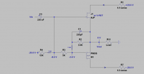
I am unsure if the attached schematic helps this discussion. I used one like it while experimenting with DEF. I do not recall reporting it; possibly because I thought it was not simple. In this example, it pertains to the condition when a large absolute difference between the Vgs of a certain R085 [or better yet SIT=2SK82] and that of IRFP9140 existed. In this schematic the example Vgs for NJF/SIT = -8V, and that of IRF9140 = -3.7 V
NPN in a common base configuration allows the input AC signal to reach the gate of the P-MOSFET in phase with it and especially not hindered [otherwise] by a large [biasing] resistor in series with its input capacitance [upsets its high frequency response].
I am unsure about possible positive/negative feedback due to this. The output signal is routed to the base of NPN/gate of P-MOSFET. It thus re-appears at the emitter of NPN in phase with the input AC signal to possibly bootstrap it. Can give NPN a bit of gain!.
The above approach is applicable to the pair 2SJ28 [SIT] and IRFP140; but with a PNP etc.
Best
Anton
Attachments
interesting , but I think impractical ..... with these resistor values (R8) , it is almost same as dead short , to previous stage
Thanks generg and Zen Mod for your replies. The attached is a concept schematic to use when a large absolute difference exists between the Vgs of a power N-JFET or V-Fet [for example 2SK82] and that of a power P-MOSFET in DEF and DEFiSIT.
The example shows a typical difference of 5 Vdc. It can readily be a larger difference in a DEFiSIT which uses a low idle current [e.g. 0.2A]; for example in a headphone application or a follower for a low power OpAmp. It follows that the value of the example [R3 =5K] will be larger.
N-JFET or SIT is a follower in its own right. Capacitor [ C1=220uF] at its source node uses the resultant in-phase output signal [Vout] to route it directly to the gate of P-MOSFET. Thus [Vin] as the new replica [Vout] essentially bypasses the high-valued resistors of the biasing string of DEFiSIT and DEF.
The aforementioned high-value biasing resistors maybe implicated [a legit or not reasoning] in degrading the high frequency performance of P-MOSFET. In the absence of the output coupling capacitor [C1], either the 5K or higher and the 3.6K are in series with its inherent input capacitance. One may argue for the potential to affect or degrade the slew rate of P-MOSFET.
generg; I look forward to your Spice simulation.
Best
Anton
Attachments
yup , we already know for that solution , and simillar
frankly , can't remember - is it from your threads , or Papa's writings somewhere , or combined
C1 is there for good reason ,doing exactly what needs to be done
in any case , one needs to take care of resulting Rin of OS stage , to not burden preceding stage too much
frankly , can't remember - is it from your threads , or Papa's writings somewhere , or combined
C1 is there for good reason ,doing exactly what needs to be done
in any case , one needs to take care of resulting Rin of OS stage , to not burden preceding stage too much
Why is Rdson important?nope
comparable Rdson with IRFP9240
didn't even look at xconductance
to be comparable with IRFP150 .........
but , you're right ...... 17S is tempting .......
🙂
maybe I'll try Babelfish M25 with IRFP150 up and IXTH26P20P down
but , you're right ...... 17S is tempting .......
🙂
maybe I'll try Babelfish M25 with IRFP150 up and IXTH26P20P down
And that reason is ? ......
C1 is there for good reason ,doing exactly what needs to be done
It looks to me like the input signal cannot affect Vgs of the IRFP9240 and it essentially becomes a constant current source.
I believe it'll work ........
anyway , at second look , maybe it is better connecting it to upper gate , instead to sources
tiny variables , best to check them in vivo
anyway , at second look , maybe it is better connecting it to upper gate , instead to sources
tiny variables , best to check them in vivo
observe currents through SIT source , mosfet source and through load as I posted in #200
red - current through 8R load
green - current through mosfet (IRFP9140)
blue - current through PapaSit
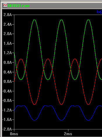
Actual circuits are similar to the sims. If you re-arrange the polarities
of the waveforms and examine the waveforms into different loads, it
becomes a little easier to see:
Current through SIT is also a function of Vds of the SIT.
With no load this circuit has AC current through SIT in opposition to
P Mosfet, that is to say out of phase.
At low impedance loads, looks more like conventional push-pull pair.
In between you see SIT working some 2nd harmonic in opposition to P.
Into 4 ohms, current cutoff of SIT occurs at about 64W peak into 4 ohms
(4 amps) where P channel clips.

- Home
- Amplifiers
- Pass Labs
- Most Greedy Boy, of them all... or (there is no) DEFiSIT of Papa's Koans