in what amplifier? if it is bias trim.pot. there should not be any trouble. to be sure,just decrease value of the resistorhi apex sir,
can i use 500r pot instead 470r pot? because in here 470r pot is not god quality.
if yes what are the changes i have to make?
in series with bias trim.pot for that 30 Ohm.
The tolerance of 500r pots and 470r pots effectively make them the same thing.
One swaps for the other.
+-10% gives a range for a 500r of 450r to 550r.
It is them adjusted to any value in that range when used as a trimmer.
One swaps for the other.
+-10% gives a range for a 500r of 450r to 550r.
It is them adjusted to any value in that range when used as a trimmer.
for apex hv25, the pot is for bias adjust.
so i have to decrease the 100 ohm resistor to 70 ohm, am i correct?
so i have to decrease the 100 ohm resistor to 70 ohm, am i correct?
Attachments
Last edited:
i changed 500r trim. for 1k trim. to get larger value of bias,with 500r it was to small. if that happens to you,set 100r resistor to a larger value,say 390r. if you get 30-50mA don't change anything.
.
have you matched all input 2n5551 and 2n5401 as close as possible? it has influence to a dc-offset
.
have you matched all input 2n5551 and 2n5401 as close as possible? it has influence to a dc-offset
don't mention it. 🙂
.
.
it is important to match all input 2N transistors as close as possible,have you done it?
.
.
it is important to match all input 2N transistors as close as possible,have you done it?
hi 44250,
i checked all hfe from 2n tranies, but readings are different from one to one,
readings hfe's 187,195,198,180,176,200 like that.
i checked all hfe from 2n tranies, but readings are different from one to one,
readings hfe's 187,195,198,180,176,200 like that.
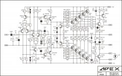
at least create a group of closest possible,say two 2N5551 of 193 and 190, with two 2N5401 of 189 and 192. second groupe could be for two 2N5551 of 173 and 170 with two 2N5401 of 169 and 172. First group would go to one chanel and second group in another chanel. be aware also that pcb is designed for 2SAxxx and 2SCxxx transistors that have different pinout. BC3xx also have different pinout compared to BC6xx -so you must check ALL transistor pinouts with scheme and apply it on pcb. i have done that and it worked from it´s first time.
Hello.
This amplifier can be powered from a +/-93v supply?
Thanks.
No, +/-80V is maximum.
hi apex sir,
i set preset to 2vdcv on 10 ohm rail 10w resitor. why the emiter resistor value is different from one one? emiter resitors showing voltage 10mv,4.5mv,15mv,0mv like this.
i set preset to 2vdcv on 10 ohm rail 10w resitor. why the emiter resistor value is different from one one? emiter resitors showing voltage 10mv,4.5mv,15mv,0mv like this.
hi apex sir,
i set preset to 2vdcv on 10 ohm rail 10w resitor. why the emiter resistor value is different from one one? emiter resitors showing voltage 10mv,4.5mv,15mv,0mv like this.
because of diferent hFE of output transistors,that is the reason why the emitor resistors are used. if they were matched (Ibe /Ie for bipolar or Ugs/Is for fet) before soldiering at pcb than this voltages would be the same and emitor resistors would not be needed.
please someone correct me if i´m wrong.
Your wrong !correct me if i´m wrong.
Can't be hFE. They are mosFETs
.mosfet-amplifier-irfp240-irfp9240
If they were BJTs, then it's variation in Vbe that leads to be variations in Ic and shows when reading the individual Vre (voltage across the emitter resistor).
For mosFET output stage it's variation in Vgs that leads to even bigger variations in Id and that shows when reading individual Vrs (voltage across the source resistor).
Last edited:
Your wrong !
Can't be hFE. They are mosFETs.
If they were BJTs, then it's variation in Vbe that leads to be variations in Ic and shows when reading the individual Vre (voltage across the emitter resistor).
For mosFET output stage it's variation in Vgs that leads to even bigger variations in Id and that shows when reading individual Vrs (voltage across the source resistor).
thank you for correcting me.
and that variation in Vgs for paralleled mosFETs is why it is absolutely important that devices be selected for very close Vgs at the target operating current for the amplifier output stage.
Last edited:
and that variation in Vds for paralleled mosFETs is why it is absolutely important that devices be selected for very close Vds at the target operating current for the amplifier output stage.
Vds or Vgs?
- Home
- Amplifiers
- Solid State
- MOSFET Amplifier IRFP240/IRFP9240