the decoupling caps are the supply, when a fast changing current is demanded. The supply rails to a remote supply are too inductive to respond to a fast change...................
As to what Tom posted in #934: the decoupling and local reservoir caps are, as the word implies, capacitors. The only thing that matter is that they can push against a hard rail, the voltage of which is unimportant. It can be ground, it can be another power rail. Since class AB only draws instantaneous current from one line at the time, you can use the power lines as terminals for the decoupling caps................
Like Twest stated
In particular you appear to be struggling with correctly accounting for inductance; that may be a useful area to prioritize for improvement.
The output from the chipamp sees two loads, the Zobel and the external load (the speaker) in series with the output inductor.
I'm with you so far.
The very fastest changes in current will go through the Zobel. It is the Zobel that must be returned to the decoupling ground.
The loop from the reservoir/decoupling cap through the LM3886 to the Zobel and back to the reservoir/decoupling cap must be a low inductance loop. Otherwise, the Zobel will have negligible effect and instability can result. You can make this loop long by various ways. Vaccuphile suggested that the decoupling ground be moved to a star ground. This makes the loop longer - both for the Zobel and for the load. In case of the Zobel, it'll impact the effectiveness of the Zobel network and in case of the load ground, it will impact the THD.
In conclusion, as both Twest and I have pointed out, it is a really bad idea to move the decoupling, Zobel, and load ground off the PCB. You can show this easily by measurements of the THD vs frequency (I've linked to the data a couple of times in this thread already). You can also simulate this rather easily using a spice simulator (TinaTI, LTspice, whatnot).
Tom
Last edited:
Tom, in some respects, isn't this a discussion of where the junction of the start ground is to be located?
You can view it that way. My argument that the star ground should be located between the reservoir/decoupling caps on the PCB. This needs to be connected to the Zobel network and load return with a low-impedance (= low resistance and low inductance) path if you want low THD and good stability.
This is possible to accomplish by careful layout of the components surrounding the LM3886 and by using a ground plane. There will be exactly one point in that ground plane where the currents sum to zero. This point will have the lowest impedance to either reservoir/decoupling cap.
Tom
This is possible to accomplish by careful layout of the components surrounding the LM3886 and by using a ground plane. There will be exactly one point in that ground plane where the currents sum to zero. This point will have the lowest impedance to either reservoir/decoupling cap.
Tom
Seems like a pretty standard way of doing it. But when you start looking at the actual implementing, things will not look so rosy. Almost seems like you want to have the signal grounding connected to it's own star before connecting to the power start. Which probably would end up having All signal grounded on one side of the PCB then the power grounded on the other side. The high current returns would go to the power ground bypassing the signal ground.
Last edited:
Yep. On the Modulus-86, I have two ground domains: Signal Ground and Power Ground.
Power Ground connects the incoming ground, decoupling ground, and load ground via a plane. This ground carries significant current.
The Signal Ground is a reference for the input and feedback grounds. This plane connects to the load ground (speaker minus) via a low-impedance path at one point only. The Signal Ground plane carries negligible current.
For a visual, see this thread (only two pages): http://www.diyaudio.com/forums/chip-amps/270206-my-take-lm3886-layout.html
Tom
And just as importantly the reference link between Signal Return/ground and Power Ground carries even less current than
The link should carry ONLY interference current and if interference attenuation is attended to at cable entries, then then is almost none left to pass along the Signal Return to Power Ground link.
This is why you can place a resistor in this link and measure no voltage across it. There is no signal to measure. This would be Joffe's HBRR.
The Signal Ground plane carries negligible current
The link should carry ONLY interference current and if interference attenuation is attended to at cable entries, then then is almost none left to pass along the Signal Return to Power Ground link.
This is why you can place a resistor in this link and measure no voltage across it. There is no signal to measure. This would be Joffe's HBRR.
I can never measure any signal across a 10r HBRR.
Is your simulation correct?
10r * 1mApk ~ 7mVac
Is your simulation correct?
10r * 1mApk ~ 7mVac
Yes, the simulation is correct.
Feedback is now a three resistor divider that is parallel with the speaker and zobel.
Feedback is now a three resistor divider that is parallel with the speaker and zobel.
Last edited:
My recommendation stands: The link between the signal ground and power ground should be low impedance.
Tom
Tom
And just as importantly the reference link between Signal Return/ground and Power Ground carries even less current than
The link should carry ONLY interference current and if interference attenuation is attended to at cable entries, then then is almost none left to pass along the Signal Return to Power Ground link.
This is why you can place a resistor in this link and measure no voltage across it. There is no signal to measure. This would be Joffe's HBRR.
I(HBRR) = I(Rfb) = I(Ri) = Vout/(Rfb+Ri+HBRR)
I can never measure any signal across a 10r HBRR.
Is your simulation correct?
10r * 1mApk ~ 7mVac
I have NEVER been able to measure a SIGNAL current across HBRR.Yes, the simulation is correct.
Feedback is now a three resistor divider that is parallel with the speaker and zobel.
Since interference is so low, I have also NEVER been able to measure an Interference current across HBRR.
The simulation cannot be correct.
HBRR has a significant voltage in my simulations as well with the LM3886 model. Using a large wattage resistor vs small wattage resistor makes a sonic difference. I was surprised as well.
In my application, I have pin7 connected to signal ground.
In my application, I have pin7 connected to signal ground.
Last edited:
I don't think the omission of the HF and MF decoupling will make a significant difference to the result. The theoretical zero impedance of V1 & V2 should account for them.
But in real life I cannot measure a signal voltage across a 10r HBRR.
That's why we can get away with adding that resistance to a potential interference current loop (when combining more than one channel) and get an attenuation of interference current in the signal circuits without and increase of interference being added to the signal voltage.
It's why the correct location fro HBRR is important. It is located outside the signal loop and it is outside the speaker loop.
I am wondering whether this is due to the LM3886 chip or not. I have seen application of 10Ohm HBRR in a class D amp, but never studied it much. Hate to draw conclusions, but I think it is important to look at instantaneous impedance paths to the ground node to control how the instantaneous current will flow. Pretty complicated considerations.
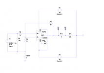
Um, guys... Have a look at Mark's schematic. The feedback current through R2, R9 has to flow through HBRR. This creates an error term which will be added to the input signal.
The current through R9 should be Vin/R9, so for 1 V RMS input, you'll have 1 mA flowing in HBRR. Even with a 1 Ω HBRR, this should be possible to measure in real life using a bench top multimeter. With 10 Ω HBRR, you should certainly be able to pick up the resulting 10 mV RMS on a scope.
Tom
The current through R9 should be Vin/R9, so for 1 V RMS input, you'll have 1 mA flowing in HBRR. Even with a 1 Ω HBRR, this should be possible to measure in real life using a bench top multimeter. With 10 Ω HBRR, you should certainly be able to pick up the resulting 10 mV RMS on a scope.
Tom
Yeh, I missed that. My sims had the input signal grounded. But it does create an error term. The input connected as Mark's schematic shows runs fine, but it can pick up noise when near cell phones.
It may "run fine" but the error term will still cause degraded performance. You'll certainly be able to measure this. Whether it's audible is another story. I suspect it will be, but I haven't performed the ABX testing to find out. A few mV out of 1 V (-50 to -60 dB error) should be audible, depending on how the error ends up summing with the input signal.
Tom
Tom
- Home
- Amplifiers
- Chip Amps
- Modulus-86 build thread