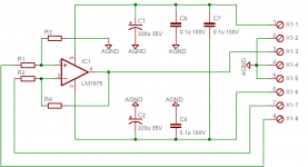
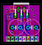
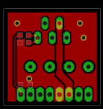
Attached is an image of the layout. It's a double sided board (red is the top layer and blue is the bottom layer) utilizing surface mount components. The board dimensions are 1 inch by 1 inch 😉
There are a number of things worth pointing out about the layout since you may miss them at first glance.
First is the use of rail to ground and rail to rail decoupling caps right next to the power pins. This is a good example of how to place the decoupling caps.
Second is the placement of the electrolytic caps very close to the power pins. This allows you to route short, low impedance traces to the power pins. Of course the physical size of the cap will dictate how short you can make the traces, so size the caps accordingly to your design requirements.
Third is the use of ground planes. If you look carefully in the picture you can see that the bottom layer ground pour connecting the electrolytic caps, the decoupling caps, and the power and speaker grounds is intentionally isolated from the other ground pours EXCEPT at the speaker ground. This ensures that all of the high currents are contained in that small ground pour AND that the other ground pours are at the same potential as the speaker ground, which is the ground reference. The 4 vias placed around the board connect the ground pours on the bottom layer to the ground pour on the top layer.
Fourth is the order in which nets are assigned to the connector. From left to right the connections are as follows: IN+, IN-, VEE, GND_VEE, GND_OUT, OUT, GND_VDD, VDD. There are 2 separate supply ground connections to accommodate a power supply with dual secondaries (this is actually my preferred type of supply). Take note that the speaker ground connection is very close to where the electrolytic caps connect to the ground plane to minimize the impedance of the ground returns.
Fifth is the position of the input and feedback resistors right near the input pins of the chip. This is good practice for any kind of sensitive inputs.
Sixth is the routing of the input signal traces away from the power supply traces as well as ground plane isolation between adjacent signals. The two input traces are purposely offset so that each is over a ground plane instead of on top of each other. This minimizes capacitance between the input nodes.
Attachments
Well, that's a pretty sweet design!
I'd also like to see room for Ci because the LM1875 is more prone to DC offset than its larger cousins.
I'd also like to see room for Ci because the LM1875 is more prone to DC offset than its larger cousins.
BWRX said:Attached is an image of the layout. It's a double sided board (red is the top layer and blue is the bottom layer) utilizing surface mount components. The board dimensions are 1 inch by 1 inch 😉
There are a number of things worth pointing out about the layout since you may miss them at first glance.
First is the use of rail to ground and rail to rail decoupling caps right next to the power pins. This is a good example of how to place the decoupling caps.
Second is the placement of the electrolytic caps very close to the power pins. This allows you to route short, low impedance traces to the power pins. Of course the physical size of the cap will dictate how short you can make the traces, so size the caps accordingly to your design requirements.
Third is the use of ground planes. If you look carefully in the picture you can see that the bottom layer ground pour connecting the electrolytic caps, the decoupling caps, and the power and speaker grounds is intentionally isolated from the other ground pours EXCEPT at the speaker ground. This ensures that all of the high currents are contained in that small ground pour AND that the other ground pours are at the same potential as the speaker ground, which is the ground reference. The 4 vias placed around the board connect the ground pours on the bottom layer to the ground pour on the top layer.
Fourth is the order in which nets are assigned to the connector. From left to right the connections are as follows: IN+, IN-, VEE, GND_VEE, GND_OUT, OUT, GND_VDD, VDD. There are 2 separate supply ground connections to accommodate a power supply with dual secondaries (this is actually my preferred type of supply). Take note that the speaker ground connection is very close to where the electrolytic caps connect to the ground plane to minimize the impedance of the ground returns.
Fifth is the position of the input and feedback resistors right near the input pins of the chip. This is good practice for any kind of sensitive inputs.
Sixth is the routing of the input signal traces away from the power supply traces as well as ground plane isolation between adjacent signals. The two input traces are purposely offset so that each is over a ground plane instead of on top of each other. This minimizes capacitance between the input nodes.
Hi BWRX,
WOW. Nice-looking layout!!!!! You seem to have been able to lay out basically everything in the most-ideal ways. Kudos!!
It looks like it's definitely time for me to start using surface-mount parts. What are the case-style designations of the ones you have used, on this PCB? Are there any slightly-larger sizes, that might be easier to hand-solder? Or is that not a big problem?
You have the LM1875 configured as a differential amplifier. Cool. Can it accept both single-ended (i.e. one side grounded, I guess) and balanced inputs? Or maybe I should just ask how it is intended to be used.
Could you explain, in more detail, how and why the grounding scheme works? I am very interested in that part. (And my eyes are getting bad-enough that it's difficult to follow, with both layers included on the PCB-layout image.)
At first glance, it looks like the 'input ground' will share a ground-return conductor with other ground-return currents, on the way to the power supply. Or maybe I'm wrong. Or maybe I'm not wrong but it works OK, somehow.
Oh wait! It's a differential amplifier! So the R3 ground SHOULD be referencing it to the 'new' output ground level. Nice.
Have you tried it, yet??!
P.S. Is there any reason that you might want to also minimize the capacitance between each input and ground, in addition to the capacitance between the two inputs?
Thanks guys. Simple circuits like these involving a chip with a nice pin out are easier to generate good PCB layouts for.
The footprints for the surface mount parts used on this board are 0805 size. Passive surface mount parts are generally classified by a 4 digit size code. This code is a combination of the length and width of the part. So when you see an 0805 size part that means it is 0.08 inches long by 0.05 inches wide. The codes are most commonly referred to using English units, but you will also see codes using Metric units. For instance, 0805 is equivalent to 2012 (2.0mm long by 1.2mm wide).
0805 is one of the most common sizes but 0603 and smaller components are widely used in a lot of consumer electronics. I don't like having to hand solder parts smaller than 0805 because it requires an even steadier hand and it is hard to control the amount of solder applied to the joint. You only need a very little amount of solder to make a good joint with surface mount components. It is also easier to read the numbers printed on 0805 size and larger components. Components smaller than 0603 generally don't have anything printed on them.
About halfway down this this page on wikipedia you can find a chart showing the standard surface mount package sizes: http://en.wikipedia.org/wiki/Surface-mount_technology
Size is of course not the only thing you need to take into consideration when selecting parts. Just like through hole parts, surface mount resistors are offered with different types of resistive elements and construction. The smaller resistors have lower power dissipation ratings and often maximum voltage ratings as well. Temperature coefficient is another parameter to keep in mind - metal film resistors have a lower tempco than the cheaper thick film types. The smaller capacitors have capacitance and voltage limits, but these are increasing as dielectric technology is improved.
gootee said:You have the LM1875 configured as a differential amplifier. Cool. Can it accept both single-ended (i.e. one side grounded, I guess) and balanced inputs? Or maybe I should just ask how it is intended to be used.
I haven't really intended it to be used in any specific manner. It could be configured as a non-inverting amp, an inverting amp, or a differential amp. What you don't see on the picture of the layout I provided earlier is that there will be exposed areas of the ground plane next to each input so that they can be bridged to ground should you want to make a non-inverting or inverting amp (these are the most common anyway). As a differential amp it could accept either single ended or balanced inputs. It would be preferred to use balanced inputs because it will work better when being driven from equal source impedances.
gootee said:Could you explain, in more detail, how and why the grounding scheme works? I am very interested in that part. (And my eyes are getting bad-enough that it's difficult to follow, with both layers included on the PCB-layout image.)
At first glance, it looks like the 'input ground' will share a ground-return conductor with other ground-return currents, on the way to the power supply. Or maybe I'm wrong. Or maybe I'm not wrong but it works OK, somehow.
Oh wait! It's a differential amplifier! So the R3 ground SHOULD be referencing it to the 'new' output ground level. Nice.
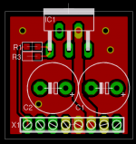
It is a little hard to see everything with both layers displayed. Attached a picture of the bottom layer so you can get a better view of the supply ground connections. It's just a copper pour connecting the supply rail grounds, the electrolytic cap grounds, the decoupling caps grounds, and the speaker ground.
Refer to my next post for comments about the ground plane on the top layer.
gootee said:Have you tried it, yet??!
Nope. I just came up with this on a whim last night, but I would like to have some PCBs made to see how the LM1875 sounds. The parts won't cost much so it won't be expensive to build up a number of these. I hadn't planned on doing a group buy of sorts but these are so simple that I could even offer to build these up (or at least populate the surface mount components) if anyone is interested.
gootee said:P.S. Is there any reason that you might want to also minimize the capacitance between each input and ground, in addition to the capacitance between the two inputs?
Ideally you want to minimize capacitance everywhere, but it is often better to have capacitance between a signal and ground versus capacitance between two signals. For this amplifier (and considering the very small size of the PCB) it's really not that critical.
Attachments
We do a lot of pc board manufacturing ,Since we are a smallish company My job are of selecting components and managing the production schedule amongst a bit of designing.
On most of our boards we still stick to 0805 and many times even 1206
Obviousely the bigger the resistor the higher its wattage , so on our analogue in parts and some digital out parts we still stick to 1206 even though that is still overkill.
Our newest designs have started to use 0603 ,but 0603 proves VERY hard to solder by hand.
And part of my job is troubleshooting and testing the boards ,and then the 0603 parts is a pain.
gootee said:Could you explain, in more detail, how and why the grounding scheme works? I am very interested in that part. (And my eyes are getting bad-enough that it's difficult to follow, with both layers included on the PCB-layout image.)
At first glance, it looks like the 'input ground' will share a ground-return conductor with other ground-return currents, on the way to the power supply. Or maybe I'm wrong. Or maybe I'm not wrong but it works OK, somehow.
Oh wait! It's a differential amplifier! So the R3 ground SHOULD be referencing it to the 'new' output ground level. Nice.
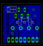
Attached is a picture of just the top layer. Look carefully at the pads of the electrolytic caps and the pads of the connector used for the supply rail grounds. I used keepouts around the pads so that they do not connect to the ground plane on the top side. This forces the high currents to stay in that small area of ground plane on the bottom side and allows the use of the top ground plane as a reference and shield. We want the ground reference potential to be the same as that of the speaker ground, which is why only the speaker ground is connected to the ground plane on the top side.
As you noted, a differential amplifier should reference to the output ground potential. That is why the one side of R3 is connected to the ground plane on the top layer.
Attachments
tangmonster said:Our newest designs have started to use 0603 ,but 0603 proves VERY hard to solder by hand.
And part of my job is troubleshooting and testing the boards ,and then the 0603 parts is a pain.
A hot air rework station is VERY handy when soldering, and almost essential when reworking, these smaller components.
Where I work we routinely use 0603 parts and the smallest components we use are 0402. I've had to solder those by hand a number of times and the tweezer tips are nearly as wide as the part! You have to be very careful when breathing or using a hot air pencil around components that small. They're extremely easy to blow right off the table or board.
BWRX said:What you don't see on the picture of the layout I provided earlier is that there will be exposed areas of the ground plane next to each input so that they can be bridged to ground should you want to make a non-inverting or inverting amp (these are the most common anyway).
Attached is a picture of the top layer showing the solder stop mask. Areas with hatch marks will not be coated with solder mask. As I mentioned above, note the two small rectangular hatched areas above the input pads of the connector. A non-inverting amp would require R2 to be grounded, so you would simply bridge that connection to the ground plane. Likewise, an inverting amp would require R1 to be grounded, so you would just bridge that connection to the ground plane.
Attachments
These little guys look great!
Any chance on a GB of these PCBs? I've got a big ol' pile of LM1875's (ahem, like 40 or so), and I've been looking for a small PCB to use them with.
Any chance on a GB of these PCBs? I've got a big ol' pile of LM1875's (ahem, like 40 or so), and I've been looking for a small PCB to use them with.
BWRX said:
A hot air rework station is VERY handy when soldering, and almost essential when reworking, these smaller components.
Where I work we routinely use 0603 parts and the smallest components we use are 0402. I've had to solder those by hand a number of times and the tweezer tips are nearly as wide as the part! You have to be very careful when breathing or using a hot air pencil around components that small. They're extremely easy to blow right off the table or board.
We recently did get a hot air station. I was a bit sceptical , but it actually does work great.
replacing that switch mode powersupply chip (u1 on the picture) with just a soldering iron is a bit hard.
One last thing , A hollow tip solder tip is THE BEST thing for surfacemount.
http://img.photobucket.com/albums/v287/tangmonster/PICT0008_2.jpg
Before ordering alot of these PCBs I would make a prototype.
The stability criteria of the amp is more critical in an inverting configuration and you have neither a dominant pole capacitor accross the feedback resistor or a Zobel network on the output to be able to adjust the stability criteria should it end up being unstable..
If you are proposing it as a general purpose amplifer it should probably have a output inductor as well. Capacitive speaker cables and even some crossovers can cause the amplifier to oscillate if there is no isolation for the amplifer from capacitance on the ouput. Experiennce suggests than arround 10nF to 100nF is the level of capacitance that normall sets off these chip amps. So if you can be sure that the load capacitance on the output will not be in this region you should be ok.
It may work without these but it also might oscillate especially as you have ground plane arround all the pins which can couple the output signal back to the input in unpredicatable ways at high frequencies which again might lead to oscillation. This amp tends to go off in the 2-5Mhz region if it is going to go unstable.
I am unsure why you are concerned about capacitnace between the input nodes. It is normal practice to keep input traces as close together as possible as this reduces the loop area from which they can pick up noise. Having said this it is unlikey to be a problem in this design. I would however move the input to a seperate connector if it was my design to keep it away from the high power recified currents comming into the local smoothing caps.
Since this is not a high speed digital design I don't think there is any benifit to having a ground plane. There may be some benifit to guard tracks arround the input connected to ground but the rest of the plane is just picking up noise from the high currents flowing in the circuits and injecting it into the ground referance. I am open to hearing a rational for the plane but my experience has been that apart from arround the low power, high sensitivity front end of amplfiers planes should not be used and even then you need to really know what you are doing to use them sucessfully.
Having said that I do like the way you have isolated the decoupling ground from the signal ground using the different layers and there is no reason for the decoupling ground not to remain as a plane as it does not couple into the signal ground.
Regards,
Andrew
For more universality I would add provision for noise gain compensation option (series RC from +IN to -IN) and for output zobel and L//R, various jumper pads etc.
Also I see no need for SMT resistors, but in case of SMT I would prefer MELF form factor.
@gfiandy
"a dominant pole capacitor accross the feedback" won't work here, we need a constant**) noise gain of >= 10
**) from about half a decade below from the Aol / noise gain intersect and upward. Can be achieved in various ways...
Regarding the GND plane, for those comparativly small currents involved (4 amps max.) a solid GND-plane is as good as it gets, IMHO
- Klaus
Howabout a bridged LM1875?
This could have a more generous soundfield, more generous gain (is more dynamics power), and more generous power output. Sort of like everything you'd want a chip amp to do. 😉
This could have a more generous soundfield, more generous gain (is more dynamics power), and more generous power output. Sort of like everything you'd want a chip amp to do. 😉
wouldn't just using an LM3875 be as good as bridged 1875s?
honestly, i dont know. havent compared, but it would just seem so.
honestly, i dont know. havent compared, but it would just seem so.
Hi Klaus,
I am sure you are right as a dominant pole on an already compensated amplifer is dodgey to say the least. I suppose I should have been more accurate and described it as a frequency compensation shelf. i.e cap and resistor. Thanks for pointing that out. I agree that compensation at the input is probably a more reliable solution though.
Still don't agree on the ground plane, I have seen them cause too many problems on power amplifers as you can't define where the currents will flow and they pick up current return paths from high current paths you weren't expecting. It probably won't make it unstable, but I don't belive it gives you the best possible solution.
Regards,
Andrew
Hi,
if you don't understand how a component works then what is the point of adding it to a working circuit?
This includes adding Ground Planes.
if you don't understand how a component works then what is the point of adding it to a working circuit?
This includes adding Ground Planes.
Hi Daniel,
adopting bridged for a chipamp does not automatically give
Going to bridged asks each chipamp to supply double the current into your selected load.
This is more likely to trigger the protection mechanisms or at least sound wrong because the combination of chipamp + PSU is stressed more highly.
adopting bridged for a chipamp does not automatically give
All Chipamps are severely limited by their peak current ability.more generous power output
Going to bridged asks each chipamp to supply double the current into your selected load.
This is more likely to trigger the protection mechanisms or at least sound wrong because the combination of chipamp + PSU is stressed more highly.
gfiandy said:I don't think there is any benifit to having a ground plane.
But with a proper poured ground plane you won't need any groundside electon pools 🙂
That was one of the features i liked about Brian's design.
I also think things like zobels should be point-to-point if required. I don't think they will be required in any of my applications so provision on the board would be wasted space.
dave
- Status
- Not open for further replies.
- Home
- Amplifiers
- Chip Amps
- Mini LM1875 design