Hi Salas.
There are no problems if I use LED 1.9V? Unfortunately I've already soldered! :-(
If used 8.3ohm resistor i get a 230ma hot-rodded version, if 9.6ohm 200ma, right?
Is there any problem for all other board component if a use 8.3ohm resistor? Any suggestion for using this value?
Thank you
There are no problems if I use LED 1.9V? Unfortunately I've already soldered! :-(
If used 8.3ohm resistor i get a 230ma hot-rodded version, if 9.6ohm 200ma, right?
Is there any problem for all other board component if a use 8.3ohm resistor? Any suggestion for using this value?
Thank you
You can use 8.3 in the negative side and 9.6 in the positive side if you got both. It will be around 200mA but you can't predict exactly from MOSFET to MOSFET sample. Its safe anyway. LEDS 1.9 are acceptable too.
ok, i understand, but i have only 8.3ohm 3w resistor at the moment. It is safe to use this value either in negative and positive side?
You suggest to make extensive use of heatsinks on mosfets and this resistors?
50va rcore 2X15W transformer is used.
Thank you for your help
You suggest to make extensive use of heatsinks on mosfets and this resistors?
50va rcore 2X15W transformer is used.
Thank you for your help
Of course you can use them 8.3 on both sides. Sinking the MOSFETS is needed at this current level and it can also be the chassis floor (use insulation pads). Not really hot yet, each MOSFET runs at about 2W. The 3W resistors can hold on their own just put them a bit high on the board for air to can pass around them. About 0.5W will burn in each of them. Because the dissipation is constant they will feel a bit more than just warm nonetheless.
*Why I wrote use 9.6 on (+) and 8.3 on (-) section if you had both is because many times the negative (IRF9240) side tends to run a little lower CCS due to usually higher VGS reading in the NMOS batches. But its not an issue in DCB1, just feels prouder for nice readings.
*Why I wrote use 9.6 on (+) and 8.3 on (-) section if you had both is because many times the negative (IRF9240) side tends to run a little lower CCS due to usually higher VGS reading in the NMOS batches. But its not an issue in DCB1, just feels prouder for nice readings.
Hi every one, I'm finish it.
But my ouput DC offset is 0.1mV and 1.5mV .
I use one on input.
Is it normal?
But my ouput DC offset is 0.1mV and 1.5mV .
I use one on input.
Is it normal?
Its still acceptable. A matter of JFETS matching. Mutually exchange places of the audio circuit JFETS pair in the 1.5mV channel. Sometimes it helps a little.
I don't understand "I use one on input".
I don't understand "I use one on input".
My input is one.Its still acceptable. A matter of JFETS matching. Mutually exchange places of the audio circuit JFETS pair in the 1.5mV channel. Sometimes it helps a little.
I don't understand "I use one on input".
R is -1.5mVAre both your output offsets negative?
i.e. -0.1mVdc and -1.5mVdc
L is 0.1mv
+0.1mVdc tells you the higher Idss device is in the CCS location.
This takes the upper device (the Follower) into the region where Id is very slightly greater than Idss.
If the +ve offset were a bit higher I would advise swapping the two devices.
Since it is so close to zero volts, just leave it as is.
This takes the upper device (the Follower) into the region where Id is very slightly greater than Idss.
If the +ve offset were a bit higher I would advise swapping the two devices.
Since it is so close to zero volts, just leave it as is.
What can I do??+0.1mVdc tells you the higher Idss device is in the CCS location.
This takes the upper device (the Follower) into the region where Id is very slightly greater than Idss.
If the +ve offset were a bit higher I would advise swapping the two devices.
Since it is so close to zero volts, just leave it as is.
My input is one and I don't connection Rotary Switch,have dependencies?
1.5mV is not the end of the world bad, pretty passable. But you could try trading places of the audio JFETs in that channel as I said. For the 0.1mV other channel do not bother.
Switch or input number has not to do with it. Just don't measure the output offset when some active device is connected on input.
Switch or input number has not to do with it. Just don't measure the output offset when some active device is connected on input.
From the measurements you have - not audible in any case BUT you might sleep better if the offset is closer to 0mv... 😉Sorry I have one question.
Is DC offset close 0mV be better???
Regards
Closer to 0mV is optimum but everything under 5mV is practically good enough. It has no impact on THD or anything else.
Ok,thanks.
And I don't use a rotary switch.
I want to use one input.
What can I connect it ??
And I don't use a rotary switch.
I want to use one input.
What can I connect it ??
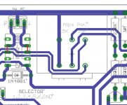
Don't populate any input relay and use input five with jumpers as the short red lines.
😀😀😀 Thanks
- Home
- Amplifiers
- Pass Labs
- Mezmerize DCB1 Building Thread