instrumentation amp.
Should you put more of the gain into the first stage?
5k+5k :200r ?
rg2 &3 all = 1k000 and you can put more effort into ensuring the ratios really are close to 1.00000:1.00000
Should you put more of the gain into the first stage?
5k+5k :200r ?
rg2 &3 all = 1k000 and you can put more effort into ensuring the ratios really are close to 1.00000:1.00000
@Ketje, no it is exactly good, U1 is used to subtract the bulk of the audio signal from the source signal.
See post #125 http://www.diyaudio.com/forums/soli...rating-class-ab-amplifier-13.html#post5098960
See post #125 http://www.diyaudio.com/forums/soli...rating-class-ab-amplifier-13.html#post5098960
@AndrewT, may be, there is a tradeoff, less gain in each step (e.g. distributing the gain) gives more GBW than most gain in the first (or second) stap. As the precision of this measurement is 1% (at a maximum) I am nit to concerned about common mode problems. Using 0.1% resistors should give enough common mode 'protection' (i think).
P.s. Simulation shows that to be able to be usable at 20kHz it needs as much speed as possible (this is why I could not find a instrumentation amplifier in the TL stock that was usable [even in simulation]).
P.s. I will do some sims and come back to this.
P.s. Simulation shows that to be able to be usable at 20kHz it needs as much speed as possible (this is why I could not find a instrumentation amplifier in the TL stock that was usable [even in simulation]).
P.s. I will do some sims and come back to this.
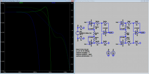
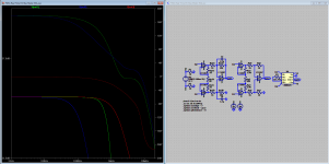
Simulation results for the INA-configuration (see also post #161 and #163) the GBW is 200kHz (distributed gain) 1MHz (single gain stage), for now I stay with the distributed (original) gain version.
Attachments
I see,you are applying a copy of the output inverted to the measuring points.Like that they are at ground level.@Ketje, no it is exactly good, U1 is used to subtract the bulk of the audio signal from the source signal.
See post #125 http://www.diyaudio.com/forums/soli...rating-class-ab-amplifier-13.html#post5098960
On one side devide (5k+1k)/1k=6 and the inverter 50k/10k=5 , not R4=60k ?
Mona
@Ketje, look at the currents in R1 and R3 (lower plot) they cancel exactly 🙂 see the residual in the upper plot (less than 6nV). Note that I connected the inputs (blue and read) to the audio signal (yellow) to show this result.
Attachments
P.s. if we have 5V at the 5k resistor then we need 1k at the 1k resistor for equal currents (and thus cancelation). 1k/5k = 200m, and 10k/200m = 50k
Question, is there anyone here with a 'valid' simulation (most preferably usable in LTspice) of the AD8421 INA?
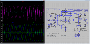
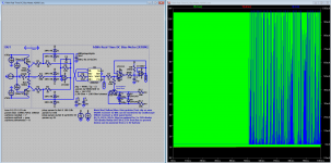
This is it, my completed version of a 'Real Time DC Bias Meter', the schema looks like buildable (I did not yet build one). Let me know what you think of it, and what may need improvement/change.
Frans, suppose the amp has appreciable DC offset and/or a complex load. Would that not compromise the 'zero xrossing'? Which I think is voltage zero xing in your scheme?
As an example, with a capacitive load, you can have zero output voltage but still appreciable output current (through an Re).
Jan
@Jan, the voltage measured is the voltage across the ballast resistors, and due to the fact that I presume that they are low inductance/capacitance, thus the current in these resistors. This is a bit complicated by the audio signal that acts as an offset for this voltage and it may/wil be influenced by the load, but, on the other hand, the signal we subtract is also under the same influence, so the subtraction should give (result into) a signal proportional to the current in the ballast resistors. Earlier I did a simulation of this and it did not show any problems.
See also post #150 Measure DC-bias in a operating class AB (or A) amplifier reactive load sample
P.s. The DC offset is a problem, the DUT best be free (at a minimum) of DC offset, I will do a simulation of this. So, first adjust the offset then measure the DC-bias.
P.p.s. Forget the p.s. I was wrong 🙂 the sim shows no 'offset' effects in the measured value
Last edited:
Question, is there anyone here with a 'valid' simulation (most preferably usable in LTspice) of the AD8421 INA?
Ok, I did get a .cir file and generated a symbol, it all seems to work. The simulation is started (for the 10kHz datapoint) but it will take a while (the simulation runs at about 700us/s 🙂 and needs slightly over 2.2s (sim time) running)
Last edited:
Simulation showing that the AD8421 is the better option.
P.s. Copy the files in the .zip file to your 'LTC\LTspiceIV\lib\sym\AutoGenerated' folder.
P.s. Copy the files in the .zip file to your 'LTC\LTspiceIV\lib\sym\AutoGenerated' folder.
Attachments
Last edited:
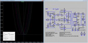
One more simulation, it shows that the device actually measures current at the current-zero-crossing.
Yes looks OK. The minimum voltage across the Re's is at zero current, independent of the actual output voltage, which is anyway compensated for, right? Neat circuit.
Jan
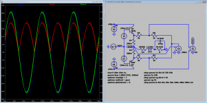
And [finally?] the AD8421 results @10kHz and @45V(90Vpp) amplifier output, this is the most difficult setting in the model.
P.s. Copy the files in the .zip file to your 'LTC\LTspiceIV\lib\sym\AutoGenerated' folder.
P.s. Copy the files in the .zip file to your 'LTC\LTspiceIV\lib\sym\AutoGenerated' folder.
Attachments

Have you simulated the effect of mismatch between R3 and R5, just to see whether your estimate of their required accuracy is correct?
An interesting corollary to auto bias/active idle monitoring is the area of determining actual peak die temp in a given thermal design/operating scenario. I implemented a small circuit to break the source connection of 1 of 8 Mosfets in a normally operating class AB amplifier circuit and momentarily bias (@1 mA) the intrinsic drain source anti parallel diode for about 10 mS so as to readout in real time the instantaneous die temp. From this exercise I could watch in real time the die temp and evaluate the actual peak dissipation occurring under actual operating conditions. Quite interesting to watch in real time the peak die temp occurring on the silicon (as observed on Oscope). No substitute for actually getting accurate readings of peak junction temp in the tricky areas of bias runaway/self heating effect(s) in paralleled device output stages (with small value degeneration resistors/ current hogging scenarios) and during fault conditions with bridged tied reactive loads.
- Status
- Not open for further replies.
- Home
- Amplifiers
- Solid State
- Measure DC-bias in a operating class AB (or A) amplifier