Hi All,
I've been playing about with this amplifier, as best I can, so I thought I'd update my findings.
Note that this is all simulator, not tried these in the metal yet - well, except for the diodes.. 🙂
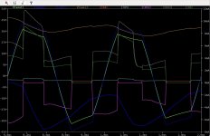
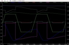
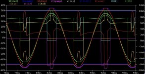
I was looking at the clipping performance, the 'edge' conditions.
From memory, pic1 is with 10R R17/18 for testing extreme conditions, pic2 is with the PSU diodes, pic3 is 1R R17/18 and a slightly smaller input signal. But I may have misremembered, so just use them for illustration.
C4 is interesting, I think it holds a voltage offset between the current mirror and the top (Wilson?) bit, the 6n8 can't hold the current when clipping, and gives a weird kink to the flat top. Another kink is solved from C8 being added, it stops that voltage reference from sagging, so the +ve clip is now nice and flat, rather than concave (worse for harmonics), and I think a little higher voltage too.
The two 1R resistors in the PSU input are for testing only, of course, the diodes on the rails are very effective, the driver is much better behaved with them: I highly recommend they are added to any design.
As for eliminating the input capacitor, C1 - ok, bad idea, it seems the tiny offset in the initial TR1/2 long tailed pair mirrors, and if that's locked to ground then sometimes 'bad things happen'...
So to summarise:
1. Power the driver seperately, or at least use schottky diodes and big caps to isolate it a bit.
2. Never remove C1
3. C4 should be 220nF, 100V.
4. Add C8, 22uF bypassing R8-D1. I'll see if this affects PSRR at some stage, but it doesn't seem to. Maybe it would be better to ground than the rail - still to investigate.
5. R11 can use 63R
I'll try out the rest of these mods when my preset's turn up, but in the meantime, hope it's been of interest.
Note - ignore the 33k R2, it's left over from my messin', should remain as 47k.
I've been playing about with this amplifier, as best I can, so I thought I'd update my findings.
Note that this is all simulator, not tried these in the metal yet - well, except for the diodes.. 🙂
I was looking at the clipping performance, the 'edge' conditions.
From memory, pic1 is with 10R R17/18 for testing extreme conditions, pic2 is with the PSU diodes, pic3 is 1R R17/18 and a slightly smaller input signal. But I may have misremembered, so just use them for illustration.
C4 is interesting, I think it holds a voltage offset between the current mirror and the top (Wilson?) bit, the 6n8 can't hold the current when clipping, and gives a weird kink to the flat top. Another kink is solved from C8 being added, it stops that voltage reference from sagging, so the +ve clip is now nice and flat, rather than concave (worse for harmonics), and I think a little higher voltage too.
The two 1R resistors in the PSU input are for testing only, of course, the diodes on the rails are very effective, the driver is much better behaved with them: I highly recommend they are added to any design.
As for eliminating the input capacitor, C1 - ok, bad idea, it seems the tiny offset in the initial TR1/2 long tailed pair mirrors, and if that's locked to ground then sometimes 'bad things happen'...
So to summarise:
1. Power the driver seperately, or at least use schottky diodes and big caps to isolate it a bit.
2. Never remove C1
3. C4 should be 220nF, 100V.
4. Add C8, 22uF bypassing R8-D1. I'll see if this affects PSRR at some stage, but it doesn't seem to. Maybe it would be better to ground than the rail - still to investigate.
5. R11 can use 63R
I'll try out the rest of these mods when my preset's turn up, but in the meantime, hope it's been of interest.
Note - ignore the 33k R2, it's left over from my messin', should remain as 47k.
Attachments


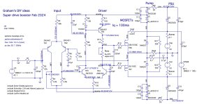
This is one of the designs I started playing with before the "Badger". (below 1).I've been playing about with this amplifier, as best I can, so I thought I'd update my findings.
The one pictured is a updated 2009 design , real simple and reliable. Good for powering Either LFET's/ or EF2/3's.
One of my builders even fired up a simpler one (below 2) to plug into the modular EF3, They work nice.
OS
Attachments
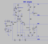
Looks good, I like the simplicity of the Maplin/Hitachi VAS, the voltage LTP into a current LTP with a 'Wilson? ish' current source on top, getting the (offset voltage for bias via RV1) drive for the MOSFET followers. Not too many transistors for the signal to get through.one of the designs
This design also allows fairly easy Local-Feedback output device designs, because the driving transistor centre (with the little preset) can themselves be wired back as the feedback source, switcheable even.
But for me 'device type selection' has drawbacks: The lateral MOSFETs are lovely, and it saves the thermo-balancing resistors too: but expensive, and slightly 'wasted' in their follower roles.... and BJTs in the VAS.. hmmm, Ok they are sort of hidden by the LTP operation, but still..
The perfect driver board for me would use FETs or MOSFETs in the VAS and driver, and allow cheap darlington BJTs for the output devices, to allow more use of the voltage rail (we lose about 10V driving the MOSFETS) a very high local feedback to be 'leveraged' in the followers to give a low impedance local feedback output stage.
For dumb followers, only gain matters, not linearity, so cheap BJTs, 'darlington'd', even slow ones, are perfect.
There's a little faffing to get adjustable offset+bias, and perhaps later, one day, the mixed opto-coupler method for auto-DC biasing, which would dispense with pesky Source/emitter resistors.
Perhaps simpler would be PTC resistors from the rails and local big PSU caps attached directly to the collectors/drains, so the thermo resistors become more part of the PSU. I.e. a slightly more integrated PSU, as amplifiers are really voltage controlled power supplies anyway.
- thinking about it, simple resistors on the PSU board between the diode bridge and the caps - to match/overrule the output device thermal runaway - would that work? Don't know.
Lateral MOSFETS are good in this respect... but even then you get music power 'fade' as they heat up, so perhaps the opt-coupler bias is the only pure way?
A Maplin/Hitachi/HH-simple stage with FETs and opto-couplers - as in the 'holy grail' thread, capable of being switched to local feedback and being able to drive darlington'd BJTs (only a little more current is needed, the Maplin design can do it) would be rather nice, and offer possibilities for very HiFi. 🙂
I'm now looking at clipping at 40Hz, as the bass is often when clips I guess.. I'm wondering if a FET VAS would be gentler for this too, tube amps always seem to have kinder clipping. Running a +60V driver rail on +50V MOSFETS is not such a crazy idea, I suspect the MOSFETs themselves would have a nicer clip - maybe I'll try this in LTspice.
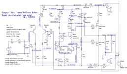
Hi All!
I had an idea when playing with the Maplin driver board in LTspice... We lose about 10V driving the MOSFETs, so a 50V rail (312W peak into 8 ohm) will generate a 40V peak drive, or 1600/8 = 200W peak into 8 ohms.
This is all burst power of course, continous depends on PSU and heatsinking etc. But music arrives in bursts, so it's Ok..
So I decided to (conditionally) feedback some of the output to the driver circuit power rail, to give it a bit of a voltage boost when it needed it. The current source and GNFB is there to tidy this up, and it's only for the loud bits...
And so you can see: a heath Robinson device on the +ve going side, just lifting the driver voltage when needed, giving 5V extra, in this attempt. 45V peak = 2025 / 8 = 253W peak into 8 ohms, so a bit more 'thump'!
This idea works toward getting a soft clipping from the MOSFETs, rather than a hard clipping from the VAS, so we'll see how it goes, and it is more components for a task perhaps better solved with a 60V stabilised PSU for the driver - but in the absence if that, I thought this maybe of interest, just4kix 🙂
I also found a cool potentiometer model, which was nice.
Attachments
Its a neat idea 👍 I tried it with a single cycle tone burst and it worked fine.
🙂
🙂
I found that at least 200 Ohm gate stoppers are necessary.
The Maplin MOSFET amplifier specified 100 Ohm resistors, enabled MHz oscillation in the output MOSFETs.
This oscillation eventually caused the Zobel network resistors to burn out.
I experimented to find the cause, and found that the specified gate resistors were too low, after eliminating all other options.
Excellent!I tried it with a single cycle tone burst and it worked fine
I'm not sure the negative side is so easy, I feel it should be, but not got anywhere near a solution yet 😀
I read this recently that got me a bit puzzled:I found that at least 200 Ohm gate stoppers are necessary
https://www.diyaudio.com/community/...plifier-design-second-try.405651/post-7598456
Saying they needed to be low values.
But for ages the wisdom was go to 220, and you again proved this. Thanks!
I ended up using 330R with the Sony heatsinks as I had slightly longer gate wires, and it seemed stable. I was wondering if that was too high! But as it works fine and 100 is too low I'll leave them at 330R.
I have 220R on the boards with the Maplin heatsink.
I'll update the schematic to 220!
I noticed a sudden increase in hum coming from the speakers, which was odd, because they were very quiet before.
The tale above came from the investigation to find the source of the hum.
It turned out to be not at all what I thought it would be. Quite a surprise, really. I mean, who'd have thought?
The tale above came from the investigation to find the source of the hum.
It turned out to be not at all what I thought it would be. Quite a surprise, really. I mean, who'd have thought?
Interesting. I think you were hearing the PSRR hum, as the MOSFETs soak up the power dealing with the RF, the PSU sags and you hear the ripple !It turned out to be not at all what I thought it would be
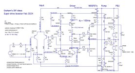
Hi all!
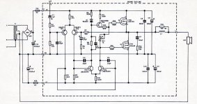
Here's the symmetrical version of the boosting driver to get that last 5V 🙂
These MOSFETs have a max Vgs of 14V, so the zener should only be 12V, which in this current flow is about 10V of power rail boost.
Bear in mind that at 5A flow (40V into 8ohms) the MOSFET Vds is 5V, even with a Vgs of 10V - I.e. these Lateral MOSFETs are 'soft', fluffy devices, not hard as a darlington BJT or a vertical, V etc MOSFET that goes down to a fraction of an ohm. At best they are 1 ohm resistors 😀
This means into 4Ohm even with the superboost you'll get 40V peaks, 8Ohm 45V, 16ohm, 48V.. etc. I.e. regardless of the GNFB trying it's best, the internal resistance of the lateral MOSFET comes into play at the extremes.
The 220uF 'push' capacitors C12, C13 can be smaller, I suspect 47uF would be fine - but the SPICE simulator gets 'unhappy' when this is tested, as I think there's a slight feedback going on that confuses it. The 'conductance matrix' solver in SPICE in combination with non-linear device models is a subject in itself, suffice it to say that SPICE cannot always model stuff that 'just works' in the bigger simulation we call our world.
I'm still looking at a way to get the clips slightly softer, it's not too bad, but would be nice if it could be completely overdriven and not spit out too much HF 😀
Also note the pump diodes have changed to 1N4148 due to their 100V BV breakdown, the schottky I first tried did 'bad things' over 60V negative. 100V should be fine I guess, but perhaps 1N4007 would be safer. 🙂
Anyway, as usual just my thoughts, I'm not really an electronics engineer by trade but then that wouldn't be DIY 😀
Attachments
I am an electronics engineer by trade, but not in audio, so I consider my efforts to be DIY.
I have a transformer that was used in a commercial MOSFET amplifier which gives +60v, +50v, 0v, -50v,-60v DC outputs after rectification and smoothing.
The VAS and input stages ran off the +/- 60v rails, and the output stages off the +/-50v rails, giving adequate drive to the output MOSFETs.
I thought about modifying the PCB of the MOSFET amplifier to accommodate separate supply rails, using a smaller auxiliary transformer for the job.
Interestingly I've only ever run this Ga28f board with seperate rails in recent years! I wanted to divorce the grounds too on this attempt, but the GNFB scuppered that.I thought about modifying the PCB of the MOSFET amplifier to accommodate separate supply rails
But I would like to add a switch, to switch between local feedback and GNFB, quite easy by I would need to add an offset control preset as the GNFB turns about 4V open loop offset into 40mV !!
When I built my original kits, back in the 1980s I heavily tinned the PCB tracks (Solder was cheap back then, even for broke schoolboys LOL), and used a single supply, later I then rebuilt them into monoblocks with soft start and split supply, but a higher driver section voltage, by 10V, would be most useful.
Not too difficult to mod a transformer either, for people without an extra winding, my Toroid had about 0.4V per turn so that's 25 additional turns per rail for the driver board, 25 turns of twin flex perhaps, I think they are would 'bifilar' anyway IIRC...
I didn't think of that, and because all my transformers are toroidal, it would be easy to do. Easier than modifying the PCB, anyway.Not too difficult to mod a transformer either
Hi all, I refined the design a little more, to remove some current spikes. D4 and D9 pull a big narrow current spike when they settle, which the 100nF caps and 39R resistors eliminate.
100uF seems to be fine for the pump reservior.
C4, the mysterious 6n8 cap across the 12k R9, doesn't in fact seem to do anything useful - as least that I can see, but causes a current spike upon clipping, this circuit seems to work better without it.
If anyone knows what it's for, please say!
R10 at 150R also reduces the current spikes, as these are MOSFETs that seems fine. Note these are not particularly big spikes anyway, and only at clipping, but I prefer them lower.
C14 is there to make sure the gates are in sync.. they are pretty close before, but I felt they should be tied. Especially as RV1 / Rbias is not necessarily so good for the sound (contacts between metal, carbon etc).
I checked the AC response for C1 at 1uF and thought it was fine, also C3 at 47uF is also fine.
I could not null out the residual 37mV at the speaker output - all suggestions welcome!
It's not the 37mV I'm worried about, it's just that I'd like to switch it to a local feedback mode, and so the GNFB can't correct the 3.5-4V offset to 37mV, in that mode - so a lower intrinsic Voffset would be essential.
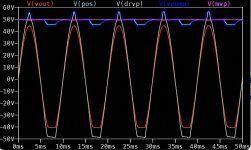
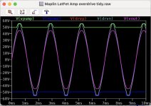
The waveform graph - note the V(out) tracking the V(drvp), at 0V they match, but the voltage diverges as drive increases - this is the intrinsic internal resistance of the MOSFET I mentioned, at 45V the driver has had to rise all the way to 55V, and even then the MOSFET sits at 45V.. Ron(min) perhaps?
So, it seems to work Ok in the simulator, but needs a lot of diodes.
I'll have a think over the next week if I want to mod the board this much, or build a sub-PSU 'pump' board on vero - decisions decisions 😀 . If I could get rid of that offset and put in a local feedback switch it would be a two-fer, i.e. 2 reasons to mod it 🙂
100uF seems to be fine for the pump reservior.
C4, the mysterious 6n8 cap across the 12k R9, doesn't in fact seem to do anything useful - as least that I can see, but causes a current spike upon clipping, this circuit seems to work better without it.
If anyone knows what it's for, please say!
R10 at 150R also reduces the current spikes, as these are MOSFETs that seems fine. Note these are not particularly big spikes anyway, and only at clipping, but I prefer them lower.
C14 is there to make sure the gates are in sync.. they are pretty close before, but I felt they should be tied. Especially as RV1 / Rbias is not necessarily so good for the sound (contacts between metal, carbon etc).
I checked the AC response for C1 at 1uF and thought it was fine, also C3 at 47uF is also fine.
I could not null out the residual 37mV at the speaker output - all suggestions welcome!
It's not the 37mV I'm worried about, it's just that I'd like to switch it to a local feedback mode, and so the GNFB can't correct the 3.5-4V offset to 37mV, in that mode - so a lower intrinsic Voffset would be essential.
The waveform graph - note the V(out) tracking the V(drvp), at 0V they match, but the voltage diverges as drive increases - this is the intrinsic internal resistance of the MOSFET I mentioned, at 45V the driver has had to rise all the way to 55V, and even then the MOSFET sits at 45V.. Ron(min) perhaps?
So, it seems to work Ok in the simulator, but needs a lot of diodes.
I'll have a think over the next week if I want to mod the board this much, or build a sub-PSU 'pump' board on vero - decisions decisions 😀 . If I could get rid of that offset and put in a local feedback switch it would be a two-fer, i.e. 2 reasons to mod it 🙂
Attachments
C8 prevents the high-side current-mirror operating at audio frequencies.
R9 makes TR3 and TR4 collector voltages unequal, and quiescent current dependant upon supply voltage, which is not good for output stage bias stability.
I used an NPN transistor instead of R9, base to 0v, emitter to TR3 collector, based on the symasym design from MikeB, which keeps TR3 collector close to 0v, and passes its collector current to the current mirror.
VAS stage current then depends upon input stage current, for which I used a current source.
These mods make it more complicated, but during testing of the original circuit, trying to set the bias, and choosing the right value for R9, while using a lower supply voltage, I noticed these problems and set about trying to solve them.
Hi! Thanks, do you mean C4?
Original Maplin schematic attached - C4 in there, 6n8.
Attachments
- Home
- Amplifiers
- Solid State
- Maplin MosFET Amplifier GA28F construction thread