
The original circuit will work best with a stabilised switching supply, like the ones I have now, but I had two transformers with different secondaries.
One was 25-0-25v, and the other 22-0-22v. Close enough to work, I thought, but this led to yet another tale, the results of which I described earlier.
Of course, If I built the kits and bought the recommended power supply I could have saved myself a lot of bother, but that wouldn't be me.
One was 25-0-25v, and the other 22-0-22v. Close enough to work, I thought, but this led to yet another tale, the results of which I described earlier.
Of course, If I built the kits and bought the recommended power supply I could have saved myself a lot of bother, but that wouldn't be me.
Ah I see, C8 was an extra capacitor I added, so I knew what that one was intended for 😀In the last diagram you posted;- This one;
But I'm baffled about the original 6n8 C4, that goes in parallel with R9, in the original Maplin schematic - do you know what that one does?
I ended up deleting it in my schematic above, as I found it just sucked current on clipping - fighting with the current source. Perhaps when not clipping it does something - but what?
With a SMPS you'd need 4 of them for best effect - 60V and 50V rails.., and if the rails are separated anyway then a Toroid becomes a good option again, as the driver stage is isolated anyway, and the extra 10V on a toroid is fairly easy to obtain 🙂
I'm still stuck between implementing the pump or adding a 60V rail. Using the existing PCB, a new 60V rail might actually be neater... just run some twin flex, a small bridge and into the caps on the PCBs... Hmmm.. Decisions!
Tending towards the extra windings now for this, then one day maybe with a custom PCB trying the other ideas...
Funnily enough I also have two spare toroid transformers like you, 22-0-22 I think, about 50-75VA perhaps. Also I have 4 spare genuine transistors from the old Sony F6B circuit - so maybe good for a local feedback amplifier project.
Small 1 Watt DC-DC converters have improved nowadays with isolation, stabilised output voltage, short-circuit protection and wide input range. A 5v-0-5v will provide 10v dc, and can sit on top of the 50vdc main SMPS output to raise the input stage rail voltage by 10v.
You have +10v dc-dc, +50v SMPS, 0v, -50v SMPS, -10v dc-dc. I'm a big fan of those little dc-dc converters, I use them a lot. Not expensive either. Much more reliable than a charge-pump.
You have +10v dc-dc, +50v SMPS, 0v, -50v SMPS, -10v dc-dc. I'm a big fan of those little dc-dc converters, I use them a lot. Not expensive either. Much more reliable than a charge-pump.
I expect C4, 6n8, across R9 is to speed up the current mirror in the original circuit. I think the whole high frequency compensation scheme is a bit messed up, with different impedances around TR3 and TR4, so what looks symmetrical cannot be symmetrical. It works with just the 27p cap around TR4.
I like the genuine ones, they run at 150kHz and have very low noise.I'm a big fan of those little dc-dc converters
Sadly the last ones I bought had fake chips, 50kHz and noisy - but in principle, yes!
Same with SMPS: the good ones are good, yes.
The bad ones however.. nightmare.
I guess it comes down to being very careful of sourcing stuff these days.
I was going to use twin SMPS for this amp, two 48 lighting or POE bricks, but after looking at the noise from my fake DC-DC converters, and looking at the shiny copper windings in my spare Toroid.. I decided to go conventional again!
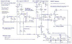
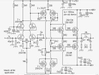
Hi all, some more testing with the Maplin PCB - this time on dual power rails, 10V more for the driver, and switcheable feedback. Yes, finally got the offset dialled out!
So most is standard Maplin, for least modding. Note the 6 x 1N4001 used in the PSU are just for simulation!!
The simulation voltage sources, all 4 of them, start with a 90 degree phase. This makes the DC .op work, so I can see the settled voltages on the schematic. If you change all those to 0 degrees, you see the voltage ramp up as the PSU starts. Some internal resistance in included in the PSU voltages.
The feedback switch is where it says NFB sw. Add a little switch in there to select the speaker out (usual GNFB) source, or with an additional 4.7k to select the Roffset. This gives identical levels into 8 ohm - the 4.7k nulls out the extra voltage the NFB sees from the driver.
As you can see, even without feedback on the speaker, the MOSFETs follow faithfully, no sweat.
So if I can figure out the number of turns needed I'll probably try this!
Attachments

Hi all!
In my gradual narrowing of 'how far to mod the Maplin', vs 'understanding how the old Maplin driver section actually worked', vs 'what about if I' mods, I've been investigating a little more.
I'm not really much further forward, although I did buy some 2n5401 and 2n5551 transistors as they are cheap and available here in the UK.
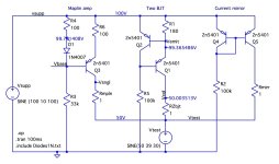
I investigated the current sources in a simulation of how constant they are in the face of a wildly varying voltage, and settled on the two BJT transistor one as my favourite.
I then realised that TR3 in the Maplin, was really acting more as a follower in this, to drive the emitter of TR4, the base of which was driven by the other side of the input TR1/2 LTP.
So in the Maplin TR4 is the main VAS, and it's current source TR5 wasn't 'that' great.
So I thought what would happen if I got rid of the follower TR3, changed TR4 for a nice MOSFET (couldn't find a 150V FET) and added another CCS to the input LTP at TR1/2.
So to me this looks like a nice clean design. The key is that the audio only has 2-3 devices in the NFB loop, so they are very fast. The CCS are 'sort of' in the path, but working to stay 'out' of the path, so any fast HV pnp will do.
Not sure what the original dissipation of the TR4 + TR5 on the board are, but suspect they run quite warm.
So how much to mod into the Maplin, I'n not sure, the CCS may be a fairly easy implant, but maybe for the ultimate I'll have to consider new PCBs.. and a new project.
Anyway, as usual, please comment and I hope the mods are interesting 🙂
In my gradual narrowing of 'how far to mod the Maplin', vs 'understanding how the old Maplin driver section actually worked', vs 'what about if I' mods, I've been investigating a little more.
I'm not really much further forward, although I did buy some 2n5401 and 2n5551 transistors as they are cheap and available here in the UK.
I investigated the current sources in a simulation of how constant they are in the face of a wildly varying voltage, and settled on the two BJT transistor one as my favourite.
I then realised that TR3 in the Maplin, was really acting more as a follower in this, to drive the emitter of TR4, the base of which was driven by the other side of the input TR1/2 LTP.
So in the Maplin TR4 is the main VAS, and it's current source TR5 wasn't 'that' great.
So I thought what would happen if I got rid of the follower TR3, changed TR4 for a nice MOSFET (couldn't find a 150V FET) and added another CCS to the input LTP at TR1/2.
So to me this looks like a nice clean design. The key is that the audio only has 2-3 devices in the NFB loop, so they are very fast. The CCS are 'sort of' in the path, but working to stay 'out' of the path, so any fast HV pnp will do.
Not sure what the original dissipation of the TR4 + TR5 on the board are, but suspect they run quite warm.
So how much to mod into the Maplin, I'n not sure, the CCS may be a fairly easy implant, but maybe for the ultimate I'll have to consider new PCBs.. and a new project.
Anyway, as usual, please comment and I hope the mods are interesting 🙂
Attachments
Globulator:
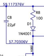
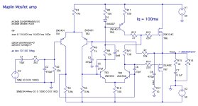
I am curious why you have C8 in the current mirror circuit circuit of the amp.
Doesn't the presence of that cap severely impede the performance of the current mirror at AC?
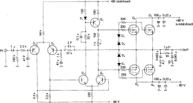
At the risk of dating myself as a fossil, I'll say I first saw this topology applied to an amplifier with a MOSFET output stage in this article while in college in the 1970s: "100 Watt Super Audio Amplifier Using New MOS Devices" from IEEE Transactions on Consumer Electronics (a professional journal from 1977).
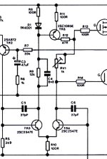
This is the schematic they featured from that long ago article. Very familiar as you can see. Hitachi engineers wrote this as they were releasing the ubiquitous lateral MOSFETs.
If I find my copy of the article, I'll post relevant pieces, unless you find it first.
😉
I am curious why you have C8 in the current mirror circuit circuit of the amp.
Doesn't the presence of that cap severely impede the performance of the current mirror at AC?
At the risk of dating myself as a fossil, I'll say I first saw this topology applied to an amplifier with a MOSFET output stage in this article while in college in the 1970s: "100 Watt Super Audio Amplifier Using New MOS Devices" from IEEE Transactions on Consumer Electronics (a professional journal from 1977).
This is the schematic they featured from that long ago article. Very familiar as you can see. Hitachi engineers wrote this as they were releasing the ubiquitous lateral MOSFETs.
If I find my copy of the article, I'll post relevant pieces, unless you find it first.
😉
Attachments
Hi!mirror
Haha, we're not fossils, I'm sure we are hydrocarbons LOL. 😀
Interesting schematic!
C8 in post #247 ? See attachment #1.
I found it tightened up the performance of square wave and clipping, in the simulation.
Without C8 the voltage at 'vasi' has pretty constant anyway, C8 making it 'more constant' helped what I saw at the output.
Later I realised that this path is not really a CCS at all (it's a 100R resistor and a diode), but that TR3 is acting as a follower, well, that's my conclusion LOL, and it was really not much of a mirror.. (see attachment #2). That 12k with the 6n8 bypass - what's that?!
So in a way C8 is connected to the reason I removed TR3 entirely on my latest mod above, and TR4 which was doing the donkey work in the VAS (is it really a MOSFET amplifier if the voltage amplification is a BJT? - discuss), I felt was not as linear as a MOSFET.
The absolute linearity of the MOSFET is less IIRC, than a FET, so for a lower voltage amp I'd use a FET there, so the voltage is amplified as sweetly as possible, tube-ily, and then the NFB has a more linear system to play with.
Attachments
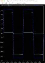
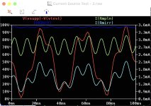
This is my little current source 'test jig' for the curious 🙂
The almost invisible blue trace is the 2 BJT case in the middle, the maplin (mpln) one on the left, and I've seen a number of people using the mirror, on the right.
In this test the supply rail is bouncing as is the test voltage, so reference and source are moving.
The almost invisible blue trace is the 2 BJT case in the middle, the maplin (mpln) one on the left, and I've seen a number of people using the mirror, on the right.
In this test the supply rail is bouncing as is the test voltage, so reference and source are moving.
Attachments
The Maplin MOSFET amplifier is based upon the one given in the Hitachi application note for their MOSFETs, and it is nearly identical to the Hitachi design.
In the application note, there is an All-FET amplifier, without any bi-polar transistors.
A search could uncover the original, which might be a useful reference.
In the application note, there is an All-FET amplifier, without any bi-polar transistors.
A search could uncover the original, which might be a useful reference.
Good idea!Hitachi application note
I found one, this is where the Maplin kit came from 🙂
Looks the same except for no resistor in L1.
I'll also have to actually read the note, as there could be useful tips there.
I also found the Hafler DH200 schematic (and construction notes), it's a BJT driver of nicely symmetrical LTPs, followers and (IMO) dubious current sources, but still interesting to see another way of driving them..
Attachments
Ah - here is the motherlode 😀All-FET amplifier
https://www.angelfire.com/sd/paulkemble/sound7g.html
Attachments
That's a different App. Note to the one I have.
A different take on it can only be good.
Not sure if the All MOS amp is the same one, Iit would take me some serious searching to find it.
A different take on it can only be good.
Not sure if the All MOS amp is the same one, Iit would take me some serious searching to find it.
I'm sure the All MOS amp is simpler in the datasheet I have, like the bipolar one but MOS.
I could be wrong, it's been a while since I saw it..
I could be wrong, it's been a while since I saw it..
There's a note at the bottom here that's interesting:
https://www.angelfire.com/sd/paulkemble/sound7g.html
I need to find a cheap, available TO220 or TO126 or similar PNP of 150V for the driver CCS in my #248 schematic
https://www.diyaudio.com/community/...ga28f-construction-thread.257488/post-7626174
The 2N4501 is not stressed in current or voltage, but dissipation is higher than I'd like with just a current of 7.75mA, which drives a nice square wave, but I'd like the option to whap it up to 10mA to see what that did.
Drive current does have a big effect on the MOSFETs, the IRF740 needed quite a decent drive too, which is why I upped the input LTP current up to 3.5mA, half of which goes to the gate.
I'll look for more app notes later, it's an interesting look back into some very nice designs.
I may also spend some time later seeing if there are better transistors for the CCS pairs, speed is everything IMO, perhaps there's a low voltage PNP which is super fast (maybe even a FET), and I need a tough HV high-hFe PNP for the current output - but probably not a darlington as I suspect they'll be slower.
It's a bit PNP heavy, perhaps the driver could be flipped and use mainly NPNs instead, easier to get perhaps.
These could actually then be added to the original Maplin design, they only need 3 connections - two to replace the resistor and one to feed in 1mA of bias. I may add one to the input LTP of the original Maplin boards, as an easy mod.
https://www.angelfire.com/sd/paulkemble/sound7g.html
Some circuits i have seen have many pairs of output devices and woefully underbiased which will limit the drive and will not give the best performance for mosfets, it is a mistake that is inherent with people believing that mosfets do not need much drive they should read the Hitachi apps notes to understand that I/P bias is needed to charge the capacitances in the gates
I need to find a cheap, available TO220 or TO126 or similar PNP of 150V for the driver CCS in my #248 schematic
https://www.diyaudio.com/community/...ga28f-construction-thread.257488/post-7626174
The 2N4501 is not stressed in current or voltage, but dissipation is higher than I'd like with just a current of 7.75mA, which drives a nice square wave, but I'd like the option to whap it up to 10mA to see what that did.
Drive current does have a big effect on the MOSFETs, the IRF740 needed quite a decent drive too, which is why I upped the input LTP current up to 3.5mA, half of which goes to the gate.
I'll look for more app notes later, it's an interesting look back into some very nice designs.
I may also spend some time later seeing if there are better transistors for the CCS pairs, speed is everything IMO, perhaps there's a low voltage PNP which is super fast (maybe even a FET), and I need a tough HV high-hFe PNP for the current output - but probably not a darlington as I suspect they'll be slower.
It's a bit PNP heavy, perhaps the driver could be flipped and use mainly NPNs instead, easier to get perhaps.
These could actually then be added to the original Maplin design, they only need 3 connections - two to replace the resistor and one to feed in 1mA of bias. I may add one to the input LTP of the original Maplin boards, as an easy mod.
The data-book excerpt above was the earlier version that included high and lower powered amp versions, a proposed PCB layout and other very useful tidbits. Later data-book versions the added the all-FET amp schematic, added some PWM amp material and deleted some of the useful tidbits. Here's a link so you can the the later version. Personally, I think the earlier version is more interesting reading. The 1977 article in the professional trade journal I referred to in my earlier post had even more useful material as well as the original schematic showing with separate supplies for the driver and output stages, recognizing the voltage swing loss incurred by driving the MOSFETs. The kemble site in earlier posts gives some good clues for research if you want to find refined and productized implementations of the basic schematic. Among other small details, I always liked the idea of using a cascode transistor in the VAS diff amp to get rid of that 12k + cap that was a kind of crude attempt to normalize the voltage across the diff amp transistors. You can see this in the schematic for the HA-7700, perhaps the last Hitachi version of that amp. Jeff Young and OS did a lot of study and refining of versions of this schematic, too. OS switched his output stage to BJTs, so you'd have to switch back to the MOSFETs. You can find Jeff's stuff in the JamJar thread and OS's stuff scattered around, probably his Mongrel thread is a good place to look for starters. This can get you started.... Eventually, you'll find your way to some Goldmund threads and Perreaux threads; they use similar topology, including the lateral MOSFET output devices.
In addition to the usual Maplin threads, that should keep you busy for a while ...
😉
In addition to the usual Maplin threads, that should keep you busy for a while ...
😉
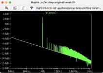
Hi all, I thought this may be of interest.
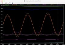
I'm learning about the FFT feature - it's on the LTspice waveform graph as 'View->FFT', done with 262144 points and 1 point smoothing. Not sure what tilts it, some time delay perhaps.
So I thought I'd look at the original driver circuit before claiming any 'improvements' 😀
FFTs are for 0.01V, 0.05V, 0.1V and 1V input.
The reason this design sounds so nice is clear to see - quiet, before the current drops off from any MOSFET, the overall performance is indeed, stunning.
Up to about 1Watt, depending upon the biasing, it's remarkably clean.
Above that the current falls off the idle MOSFET and the GNFB has a mad scramble, thus pushing all of the harmonics up the frequency scale - but still quite low. The GNFB loop is quite short, IMO the reason it works well here.
Then at 1V input, 30V output it's a big fuzzier but still pretty clean.
I.e. distortion rises with level which is natural, and at the most popular listening levels, <1W, it's only a tiny bit of 2nd, so very sweet.
I suspect the higher the bias, the cleaner the sound as it does seem to be the crossover into class B that brings it out of the sweet spot - so perhaps much of the quality is simply down to a very very clean class A region with a graceful degredation into class B, more subtle with for BJTs.
Attachments
-
Cordell-Models.txt23.5 KB · Views: 56
-
Maplin LatFet Amp original tweak.asc11.8 KB · Views: 75
-
 Maplin original at 1.0V.jpg87.7 KB · Views: 117
 -
 Maplin original at 0.1V.jpg79.2 KB · Views: 78
 -
 Maplin original at 0.05V.jpg70.2 KB · Views: 72
 -
 Maplin original at 0.01V.jpg74.8 KB · Views: 97
 -
 Maplin original FFT testing.jpg169.4 KB · Views: 114
 -
Diodes1N.txt989 bytes · Views: 66
Firstly are you using an FFT window? Usually essential unless your signal exactly repeats in the duration of the run (which is always going to help anyway). The flattop window will give accurate peak heights, note, other windows can give a dB or two of error due to scalloping.I'm learning about the FFT feature - it's on the LTspice waveform graph as 'View->FFT', done with 262144 points and 1 point smoothing. Not sure what tilts it, some time delay perhaps.
There are some options for more accuracy in internal calculations that help FFT's come out better:
.options plotwinsize=0
.options numdgt=10
Often it pays off to hide the first bit of the simulation from the output in case there's a start-up transient which will add low-frequency energy. So for instance
.tran 0 11ms 1ms 2e-8
(which samples from 1ms to 11ms, giving a run of 10ms with any issues of startup transients chopped off the front.)
- Home
- Amplifiers
- Solid State
- Maplin MosFET Amplifier GA28F construction thread