I may be misunderstanding something here. But aren't the ZV9 and F3 configured as you describe? With the cascode FET's gate voltage being derived from it's drain
From eyeballing the curve plots:The Vg steps are from -1.6V to +1.2V by 0.2V.
- Current gain (fixed Vds) is about 1 A/V both for the LU alone and the modulated cascode
-Voltage gain (fixed Id) is about 1 V/V for the LU alone and about 10 V/V for the modulated cascode.
Why/how does the IRFP240 contribute to the voltage gain?
The ZV9 and F3 derive the DC voltage of the cascode gate from voltage divider between the cascode drain and ground. There is a capacitor to ground the keep that voltage constant.
In my modulated cascode, there is no such capacitor.
In my modulated cascode, there is no such capacitor.
My error. When I looked at the schematic I thought I saw an extra resistor which would have accomplished that.
Instead the voltage modulation occurs from voltage variation across the Source resistor of the Jfet.
Instead the voltage modulation occurs from voltage variation across the Source resistor of the Jfet.
1. What would be a simple but good way to achieved the 4.9V reference for the IRFP240? A driver resistor wie a Zener diode? A CCS+resistor across the Vd supply?
2. How will a different voltage value change the operation of the whole circuit?
2. How will a different voltage value change the operation of the whole circuit?
That 4.9V voltage isn't magic, but it affects the quiescent Vds operating point of the LU1014. A zener would work or you could use a resistor with a fairly large capacitor across it in series with the rest of the voltage divider chain.
Wow Lynn, this is interesting!
Here's an example of an actual amplifier.
I've been listening to what I call a LuAmp for a while. It's NP's Zen Variation 8 with choke loading instead of the light bulb loading (Choked F3?).
Look at what the modulated cascode does. Sim is 1W, 2W, 4W, 8W

It lowers the distortion by half and is more H2, until H3 rises at 8W. Also notice the phase of the H2 is different. I would flip speaker polarity to get -H2 after this Triode mod.
I had to fiddle with to find a capacitor value that worked for my existing bias pot arrangement.
Thanks for the work on this triode idea.
Cinco
Here's an example of an actual amplifier.
I've been listening to what I call a LuAmp for a while. It's NP's Zen Variation 8 with choke loading instead of the light bulb loading (Choked F3?).
Look at what the modulated cascode does. Sim is 1W, 2W, 4W, 8W
It lowers the distortion by half and is more H2, until H3 rises at 8W. Also notice the phase of the H2 is different. I would flip speaker polarity to get -H2 after this Triode mod.
I had to fiddle with to find a capacitor value that worked for my existing bias pot arrangement.
Thanks for the work on this triode idea.
Cinco
Attachments
Gain = - ( ∆ Vout / ∆ Vin ) = - ( (35 - 20) / (1.0 - -1.4) ) = - (15 / 2.4) = -6.25x [16dB]So what is the gain ?
Load line = (35 - 20) / (2.2 - 0.2) = 15 / 2 = 7.5Ω
(approximations)
Attachments
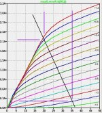
A lower output impedance: Zo = (42 - 20) [V] / (1.8 - 1.3) [A] = 22V / 0.5A - 44Ω
As a 'pentode' (common source circuit) 40 / 0.1 = 400Ω (visual approximation)
As a 'pentode' (common source circuit) 40 / 0.1 = 400Ω (visual approximation)
No, as an amplifier (common source circuit).
It resembles a V-fet, the drain is a low impedance amplifying output.
The curves bends wrong compared, and there is less linearisation.
The much sought-after electronic holy grail.
It resembles a V-fet, the drain is a low impedance amplifying output.
The curves bends wrong compared, and there is less linearisation.
The much sought-after electronic holy grail.
Some questions regarding the equations:In my previous post showing the "extended-triode" transconductance, I forgot to include the equation for unmodulated (pentode) mode:
General: µ = gmJ1Rp -> 'Rp' is plate resistor, plate resistance, load?
Modulated cascode equation: ... 1 / ( gmM1µ) ... -> to which 'M1' is referred here?
Unmodulated (pentode) cascode: ... 1 / (gmM1) ... -> same which 'M1?
In the drawing, both resistors connected to the mosfet gate are calculated with respect to 'Rk'. What is this 'Rk'?
It is well known that active semi's has a low output impedance (like vacuum triodes) in the ohmic region (Vds ≤ Vgs cq Vce ≤ Vbe), but are hardly useable in that limited voltage range. Only J-fets are used this way as amplitude regulators in eg wien bridge oscillators.
This is a very smart solution and application to 'fold' this much elegant ohmic behaviour into more useable output voltages!
But alas, the curves are 'mirrored' in respect with true vacuum triodes. However, this might work in HV triode circuits too!
You may coin it as the 'lhquam-cascode' ("cam-casc").
The equation should have been:
µ = gmJ1 x Rd, where Rd is the FET counterpart to the triode plate resistance Rp.
In the term gmM1 x µ, gmM1 refers to the transconductance of the MOSFET.
Rk is an overall resistance between the M2 drain and the Vcasc voltage source. Rk=900R in post#1.
My original objective was to create a 3-terminal circuit that extends the Vds range of the LU1014D and preserves its triode-like behavior. I will soon post a more complete explanation.
Rd is the load, {RL} in #12, ok.
gm is the transconductance of the mosfet, that's known. But M1 is not present. M2 is.
Rk is R3 + R4, ok.
Your objective has been reached. Chapeau.
gm is the transconductance of the mosfet, that's known. But M1 is not present. M2 is.
Rk is R3 + R4, ok.
Your objective has been reached. Chapeau.
- Home
- Amplifiers
- Pass Labs
- LU1014D Modulated Cascode