If I talked to Bob he would see his wrongness. Trust me he is a good buddy.He says measure VTO at 1% of Idss.
Have you tried that?
To do justice to the author: I shortened the recommendation given in Cordell's book for creating a jfet model.
He recommends to measure Vgs that brings Id to 1% of Idss and to plug this value in the spice model as VTO.
Then go fiddle with beta and lambda to fit your I-V characteristics.
This program could mean that you populate the model with four measurements: One for VTO, one pair for beta and one pair for lambda. The two pairs can share one (Vgs, Vds, Id) point.
The 1m$ question is where to place those measurement point to make the model most relevant for the intended purpose.
The 1m$ question is where to place those measurement point to make the model most relevant for the intended purpose.
It might be more practical to just implement a known better quality model. It seems modeling in commonly available simulators tends to lag SOTA by 10 years or more.
FWIW, to determine the pinch voltage, the usual recommended lab procedure is to measure Id vs. Vgs at a very small Vds (so in the jfet linear region), determine the linear region of the Id-Vgs curve (so make sure the subthreshold part is avoided, also avoiding high current effects, which are usually saturating the drain current at high Vgs) then extrapolate this linear region to Id=0.
From post #10
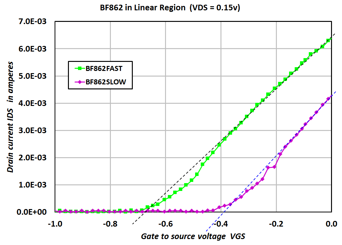
fast: -0.672V
slow: -0.389V
does this have to be corrected for the 38mV mismatch?
From post #10
fast: -0.672V
slow: -0.389V
does this have to be corrected for the 38mV mismatch?
Not sure where 38mV is coming from. Also no idea why you call those devices "fast" and "slow". They seem to have about the same channel conductance (which makes sense).
Mark pointed out that his curve tracer has an offset.
And he dubbed them fast an slow. Kids need names, call them green and violet if you like.
(...)
You can see that my curve tracer's channel-2 has a 38mV offset: when I tell it to output -200mV, it actually puts out -162mV.
And he dubbed them fast an slow. Kids need names, call them green and violet if you like.
EDIT - someone posted this short but concise IEEE paper for free describing both problems ...
http://dlia.ir/Scientific/IEEE/iel1/16/2015/00055768.pdf
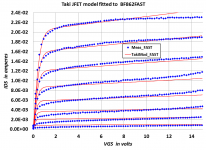
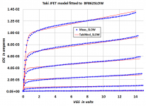
Thanks Scott! Sorry for the delay, I only got around to fitting that model to the Worst Case BF862 measurements, this morning. I came up with the following fitted values of Taki's parameters:
Code:
Taki model          BF862SLOW     BF862FAST
parameter           value         value
============================================
IDSS               +8.525E-3     +1.857E-2
VP                 -0.510        -0.822
ALPHA              +1.373        +1.458
LAMBDA +2.798E-2 +1.425E-2It's a darn shame the current release of LTSPICE doesn't include the Taki model or any of its cousins!
_
Attachments
Last edited:
I still believe you should get to grips with modelling a real middle-of-the-road device first and then see how you fare on the freak devices.
I have chosen a different design approach, one which requires worst case models only. If you don't care for this particular method, please feel free to choose a design approach of your own. If your procedure calls for fitting JFET models yourself, the good news is that the job isn't difficult. Depending on what equipment you already own, it may not be expensive either (see post #13).
Sure,
but obviously your fast device refuses to follow either the standard LTSPICE or Taki's predicted behavior for variation of Vgs.
but obviously your fast device refuses to follow either the standard LTSPICE or Taki's predicted behavior for variation of Vgs.
Your welcome, most of my IEEE downloads are not for posting since we pay for them. One more thing LTSPICE does support the "B" parameter IIRC which allows a better fit if the device is not exactly square law. Simply take the data in the first region in the linked paper Vp is still the extrapolated intercept but if the slope is not 1/2 you can use the B parameter to fudge it. Someone should go through the exercise though I find the low noise FET's folks really worry about are very close to square law.
Since y'all are close to owning LTSpice, anyway you can beat some heads for more advanced transistor models? 😉
(Thanks, by the way for the paper)
Since y'all are close to owning LTSpice, anyway you can beat some heads for more advanced transistor models? 😉
(Thanks, by the way for the paper)
I've been assured it will be well supported for MOS and Bipolar devices at least. We had to do a level 3 JFET for GaAs designs, don't know if the code plugs right in. From my discussions years ago LT took and built upon the free Berkeley code. Ours was done from scratch decades ago and has a lot of different features.
Very cool and good to know!
Many of the newer simulation tools are well beyond my pay grade, but it'll be good to have some more sophisticated transistor models (and the ever-hopeful better IC models).
Many of the newer simulation tools are well beyond my pay grade, but it'll be good to have some more sophisticated transistor models (and the ever-hopeful better IC models).
I tried the Sansen & Das JFET model just now; it was reference [10] of the Wong paper that Scott posted. I couldn't get it to fit very well at all; it was much worse than the Taki (hyperbolic tangent) model fit shown in post #48. Taki model was equation (1) of the Wong paper.
Wong cautions that the parameter "K" in Sansen/Das's model is "crucial to the smoothness in the transition region" and maybe I'm not fitting it properly. But after several dozen restarts from different initial points, I haven't gotten S/D results that are anywhere near as good as Taki. Go figure.
Wong cautions that the parameter "K" in Sansen/Das's model is "crucial to the smoothness in the transition region" and maybe I'm not fitting it properly. But after several dozen restarts from different initial points, I haven't gotten S/D results that are anywhere near as good as Taki. Go figure.
Last edited:
I tried the Sansen & Das JFET model just now; it was reference [10] of the Wong paper that Scott posted. I couldn't get it to fit very well at all; it was much worse than the Taki (hyperbolic tangent) model fit shown in post #48. Taki model was equation (1) of the Wong paper.
Wong cautions that the parameter "K" in Sansen/Das's model is "crucial to the smoothness in the transition region" and maybe I'm not fitting it properly. But after several dozen restarts from different initial points, I haven't gotten S/D results that are anywhere near as good as Taki. Go figure.
This is a tough problem, I admire your energy. I could send you Taki's original paper, his examples are the Toshiba JFET's close to everyone's heart and his curves fit very well.
Attachments

Last edited:
Thanks, Scott. I've already got Taki's paper in pdf format. It's on those JSSC DVDs that Tim Tredwell of Kodak made for the SSCS around 2005. Gotta say they are sometimes a lot more handy than logging into IEEE Xplore Digital Library. Sansen and Das's paper is on the same set of discs. On the other hand, the Wong paper that you uploaded, was from Trans.E.D. which is not on the discs. Thanks again for that.
edit- fixed typo in acronym. that nobody would have noticed anyway.
edit- fixed typo in acronym. that nobody would have noticed anyway.
Last edited:
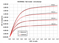
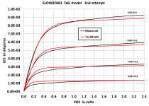
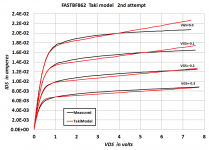
Taki revision 2
I had another go with the Taki model, to see what happens when I place more emphasis on tightly fitting the linear region (low VDS). Even though the Taki model is not yet available in LTSPICE. I also found a way to cancel the 38mV offset in the curve tracer's VGS; thus the plot labels are even multiples of 100 millivolts.
The JFET's linear region can be fitted rather well (Figs 1 and 2), but this leads to larger mismatches in the saturation region (Figs 3 and 4). The bumps and wiggles are artifacts of the low cost curve tracer, not of the model equations.
I think that's about all I've got on this one. Never did succeed getting the Sansen and Das equations to fit.
Attachments

- Home
- Amplifiers
- Solid State
- LTSPICE models of worst-case BF862 JFETs