So I got a note from Digikey saying the BF511 was suggested replacement for the EOL BF862. Does anyone have models for this one yet? Seems like a much lower current JFET?
BF511,215 NXP USA Inc. | Discrete Semiconductor Products | DigiKey
BF511,215 NXP USA Inc. | Discrete Semiconductor Products | DigiKey
Last edited:
I wouldn't replace the BF862 with any other JFET from NXP, even if there was a suitable replacement. Just think about why they would discontinue the BF862 just a couple of months after they still advertised them in a new RF Manual (20th ed.) as the preferred part (bold typeface).
My guess is this:
When NXP split off their business of discrete and logic parts to the new company Nexperia in 2016, they also sold the respective factories. Somehow, the JFET product line managed to stay with NXP, presumably because they're officially part of the RF portfolio, which remained with NXP. However, they were most probably manufactured in the same fab as the other discrete parts, like small signal BJTs.
Given the specialist status and relatively low turnover of JFETs, I imagine they have simply been overlooked by the management, and when they found out about it some time during the first half of 2017, they realized that they couldn't produce the things any longer, because the fab was now with Nexperia.
They would have to go to Nexperia and strike a deal to have them continue producing the JFETs. I guess they went the easier route and decided to discontinue the affected parts.
This of course would mean that they will eventually discontinue all JFETs. It probably depends on the amount of stock they have left.
They will probably want to handle this in a low key fashion, because they are in the process of being bought by Broadcom, so the management probably want to avoid creating the impression that they have made a mistake. It might have an impact on their compensation package when the merger goes through.
Perhaps someone with closer connection to NXP or Nexperia can share some insight that confirms or contradicts my conjecture.
It is a pity for the BF862, because there isn't a good replacement. OnSemi have shown some activity in the JFET scene in the last years, and new parts are being introduced. Hopefully they come up with something to match the BF862.
Hello, I'm sorry for resurrecting this old thread, but, lately, I've been investigating a little bit on various JFET Spice models, the ones included in LTSpice, the ones available at LTWiki and the ones available at InterFET website and, to my great surprise, I've discovered it is really really difficult to find a "trustable and reasonably accurate" JFET models, BF862 included (apart from the ones made by Mark Johnson, the author of this thread: they seems to be really well made instead!)
More specifically:
1) I discovered a good 80-90% of the models included in the default LTSpice jfet library have really high values (greater by a factor of 10 millions!!) for the Af parameter (exagerating flicker noise really a lot, example: J113), or, on the contrary, have Af = 0 (hence, as far as I undestand, ignoring flicker noise completely)
2) InterFET library, on the other hand, seems to suffer of wrong Alpha and Vk values, being a lot of the jfet in their library having Alpha = 1 and Vk=1 (that seems the default values for Orcad PSpice, while LTSpice default is zero for both)
This makes the drain current of their models hugely dependant on Vds, hence they behave more like a resistor/forward biased diode than a transistor! (at least in LTSpice)
I already reported the anomaly described in the 1) to AnalogDevices and LinearSystems: they generated a case for my request and are looking at it.
I reported the 2) to InterFET but they didn't give me any feedback yet.
On the 2) I would be really grateful to anyone who will be so nice to explain why and how Alpha and Vk parameters can have so much strong impact on the jfet model behaviour. On this matter, I found another BF862 model on DIYaudio forum, here:
LTSPICE model for your BF862 JFETs
The latter is made by the user ElFishi and it behaves a lot like InterFET models: drain current is immensely dependant on Vds! This doesn't happen on the models made by Mark Johnson and the major difference between the ElFishi model and Mark Johnson models are Vk and Alpha!
I put them below for convenience:
Please, could someone give some deep insight on the reason of the very different behaviour of these models (As I said, I guess Vk and Alpha are the suspected parameters)?
More specifically:
1) I discovered a good 80-90% of the models included in the default LTSpice jfet library have really high values (greater by a factor of 10 millions!!) for the Af parameter (exagerating flicker noise really a lot, example: J113), or, on the contrary, have Af = 0 (hence, as far as I undestand, ignoring flicker noise completely)
2) InterFET library, on the other hand, seems to suffer of wrong Alpha and Vk values, being a lot of the jfet in their library having Alpha = 1 and Vk=1 (that seems the default values for Orcad PSpice, while LTSpice default is zero for both)
This makes the drain current of their models hugely dependant on Vds, hence they behave more like a resistor/forward biased diode than a transistor! (at least in LTSpice)
I already reported the anomaly described in the 1) to AnalogDevices and LinearSystems: they generated a case for my request and are looking at it.
I reported the 2) to InterFET but they didn't give me any feedback yet.
On the 2) I would be really grateful to anyone who will be so nice to explain why and how Alpha and Vk parameters can have so much strong impact on the jfet model behaviour. On this matter, I found another BF862 model on DIYaudio forum, here:
LTSPICE model for your BF862 JFETs
The latter is made by the user ElFishi and it behaves a lot like InterFET models: drain current is immensely dependant on Vds! This doesn't happen on the models made by Mark Johnson and the major difference between the ElFishi model and Mark Johnson models are Vk and Alpha!
I put them below for convenience:
Code:
*Models by Mark Johnson at DIYaudio, fitted from real measurement of 100 *BF862 transistors, they seems to behave really really well!

.MODEL  FASTBF862  NJF( VTO=-8.238E-1  BETA=2.812E-2  LAMBDA=1.133E-2 IS=6.82E-14   N=1.235
+                       ISR=3P         NR=2           RS=0.5         RD=0.5         BETATCE=-0.5
+                       VTOTC=-2E-3    ALPHA=1E-3     VK=6.0E2       M=0.6          PB=0.5
+                       FC=0.5         CGS=9.5P       CGD=7.5P       KF=8.75E-17    AF=1
+                       MFG=NXP)

.MODEL  SLOWBF862  NJF( VTO=-5.083E-1  BETA=3.394E-2  LAMBDA=2.426E-2 IS=1.19E-13   N=1.255
+                       ISR=3P         NR=2           RS=0.5         RD=0.5         BETATCE=-0.5
+                       VTOTC=-2E-3    ALPHA=1E-3     VK=6.0E2       M=0.6          PB=0.5
+                       FC=0.5         CGS=9.5P       CGD=7.5P       KF=8.75E-17    AF=1
+                       MFG=NXP)

*Model by  ElFishi at DIYaudio, measured the device characteristics of 14 *JFETs and fitted the LTSPICE model for the saturation region.
*STRANGE BEHAVIOUR: THE DRAIN CURRENT IS HUGELY DEPENDANT ON Vds!!!

.model BF862_ElFishi NJF(beta= 0.049998 VTO= -0.5967 lambda= 0.036629 Rs= 7.234 Is= 9.36E-14 N= 1.245 Betatce=-.5 Vtotc=-2.0E-3 Isr=2.995p Nr=2 Xti=3 Alpha=-1.0E-3 Vk=59.97E1 Cgd=7.4002E-12 Pb=.5 Fc=.5 Cgs=8.2890E-12 Kf=87.5E-18 Af=1)
Please, could someone give some deep insight on the reason of the very different behaviour of these models (As I said, I guess Vk and Alpha are the suspected parameters)?
I only measured the zero-hertz ("DC") behavior of BF862 devices, and I only fitted the drain current versus gate voltage (and drain voltage) parameters VTO, BETA, LAMBDA , and the gate-to-source junction diode parameters IS, N. These are DC parameters. It's all explained very thoroughly in post #1 of this discussion thread.
All of the rest, I simply copy-and-pasted from some SPICE model or another, I don't remember which, because I wasn't interested in those other parameters at that time.
I invite you to follow the same approach that I took: (1) identify the parameters that you really, REALLY care about; (2) obtain a population of semiconductor devices to measure; (3) obtain the necessary test equipment to measure those devices in the regime you really, REALLY care about; (4) measure the parts and capture the data, yourself; (5) perform linear regression or if necessary, nonlinear regression, to extract the parameter values from the measured data; (6) victory!
As you have seen, it may not be wise to rely upon SPICE models created (or just copy-and-pasted) by complete strangers on the internet. Their region of interest may not overlap yours, and their idea of "good enough" may not agree with yours.
Best wishes,
Mark Johnson
I only measured the zero-hertz ("DC") behavior of BF862 devices, and I only fitted the drain current versus gate voltage (and drain voltage) parameters VTO, BETA, LAMBDA , and the gate-to-source junction diode parameters IS, N. These are DC parameters. It's all explained very thoroughly in post #1 of this discussion thread.
All of the rest, I simply copy-and-pasted from some SPICE model or another, I don't remember which, because I wasn't interested in those other parameters at that time.
Hello, kind sir. I need to use such a nice intro, because you have helped people a lot.
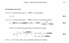
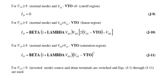
I wanted to share with the world my experiences with analysis and such. So, first, the fitting should not be done to a whole data set, but only for the one which the equations are relevant in simulating.
Example, you could see the lower current BF862 to start having an inflexiion upwards at higher voltages. That one zone should have been excluded from the calculation of the output conductance, and thus Lambda, since it is caused by an entirely different effect, the ionisation, in simulation of GASFET, under alpha, Vk and B. (alpha Ionization coefficient, Vk Ionization knee voltage, B Doping tail parameter) Basically, think of everything as some regions, and you do the best fit for only that region. If the inclination of the data and of the model are different (different Early voltage, that is g(os), that is LAMBDA), they are not the same thing. Ideally, you would want the model to be so good as to represent all the process variations by changing only a single parameter, the VTO.
Of the Vto, treshold voltage, that one should also be selected not to be smaller than the real one... especially not measured at some high current, such as 100 000 000 picoamperes, because, the simulation is ordered to drop the Id to zero once below the Vto gate control voltage. What's going on here? For some people (Me, specifically), the femtoampeters are VERY important, or at least balancing them out. And the datasheet varyingly specifies the "VTO" at 1uA, 10uA or some other current. That is for practical reasons, for measuring picoamperes takes a LOT of time.
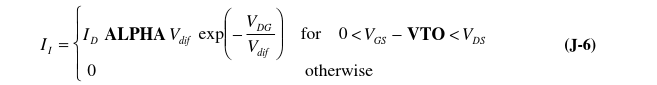
There is some strangeness going on from what I read about people reporting the difference of using a B parameter and not using it, namely, that without that parameter, a different equation set is used. In other words, since the B parameter truly invokes much more realistic conditions simulation, there is no other option than using it. There is a simple explanation: at high DS voltages, the current flowing trough the channel will cause the same effect as injecting current into the gate. that means for accurate simulation, the parameters should be used. I think the equation set for the B-doping tail parameter, is the same as in the GASFET Level2, as there is no other equation using the B parameter, even.
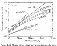
What else: internally, BF862 is composed of two identical antiparallel-connected JFET transistors, so that D1-S2 and D2-S1 are connected, so any model not using Rd and Rs and Cgd and Cgs of identical values is going to miss some important aspects. Of course, in simulating just a limited operating area, it may not come up.
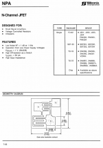
What else have I learned: It was discovered long, long ago, with the National Semiconductor P51 process (well, discovered likely before, but this one has a record of being made eons ago) that combining JFET transistors of varying treshold levels and W/L ratios will lead to lower distortion. You may see the very sharply turning switching JFET transistors of Motorola/ON datasheet that have different markings and such. While the sharp breakover is interesting as a constant current source, it's not universally desirable.
The 1976 Siliconix datasheet has a uniform structure for the J202, but the 1989 had a 2-transistors in parallel system used. (change happened sometimes earlier)
Implications? If you can't do a fit in any way, the real transistor could be composed of several different types anyway and you would do better not to torture yourself and do the same, connect two+ models in parallel. A hint: one of the transistors has a lower treshold than the other one.
You can also see that the ionisation is important in simulating the gate current, or put in another way: seeing the gate leakage in datasheet or in reality quickly allows you to determine the ionisation parameters, if only as some starting values. In case of teh siliconix SST201, SST202 (J201, J202, etc), it starts at only 15V. This is easy to verify in simulation and it can possibly lead to good starting values for those parameters.Of course, one blink of an eye into the equations is always healthy.
Attachments
-
 GASFET Level2.png22 KB · Views: 126
 -
 JFET drain current.png18.5 KB · Views: 129
 -
 JFET gate current addition Ii.png4.9 KB · Views: 117
 -
 Siliconix NPA 1989 p1.png32.1 KB · Views: 106
 -
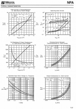 Siliconix NPA 1989 p2.png62.8 KB · Views: 119
 -
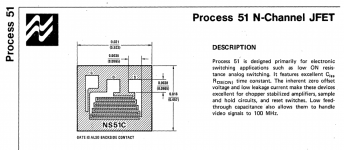 P51.png39.2 KB · Views: 150
 -
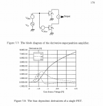 Low distortion superposition.png16.5 KB · Views: 168
If you are really interested in low gate current, you might find
this here interesting:
< https://arxiv.org/pdf/1708.06311.pdf >
They use the Interfet IF3602 which has huge area and is IMHO overhyped.
What is different in the 2 halves of the BF862? Somewhere in my 50 TB
of data I have a chip photo of it and it did not look very special.
BF862 is said to get serious channel ionization @vds > 5V; I had never
problems thanks to cascoding @ 3V Vd.
Does anybody out there have an ADS design kit with the fashionable
JFETs like BF862, 2SC170, CPH3910 etc? Yes, I could use the spice
parameters, but I'd like something tested. I'm still at the ADS novice level.
Weird: this was the first time I got a thread update email in maybe 10 years here.
Cheers, Gerhard
If you are really interested in low gate current, you might find
this here interesting:
< https://arxiv.org/pdf/1708.06311.pdf >
They use the Interfet IF3602 which has huge area and is IMHO overhyped.
What is different in the 2 halves of the BF862? Somewhere in my 50 TB
of data I have a chip photo of it and it did not look very special.
BF862 is said to get serious channel ionization @vds > 5V; I had never
problems thanks to cascoding @ 3V Vd.
Does anybody out there have an ADS design kit with the fashionable
JFETs like BF862, 2SC170, CPH3910 etc? Yes, I could use the spice
parameters, but I'd like something tested. I'm still at the ADS novice level.
Weird: this was the first time I got a thread update email in maybe 10 years here.
Cheers, Gerhard
The useful (=cheap) types at the moment are: MMBF5103 (and maaaaybe MMBF4093), 2SK3557-6, CPH3910, MCH5908G (=2x 3557-6), CPH5905 (3557 cascode with a good NPN)
MMBF5103 and MMBF4093 are supposed to be National Semiconductor Process 51 transistors.
I will put more research online (hopefully), but I got to get used to this interface.
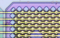
BF862 is brilliant, it has about 5.6 milimeter channel WIDTH, uses an actual gate-grid, the two halves are identical, antiparallel connected. The channels are short. Also, uhh..
I forgot.
anyway, what you need is to get as close to the theoretical line of transconductance as possible. Imagine noise staying the same, but the amplification differs, the relative amount of noise would be smaller with higher transcondctance. Of course there are deuteriation tricks to lower the noise during manufacture, but the basic architecture always remains. And BF862 offered unparalleled gate had channel width at the time. And 2-micrometer channel width? Are you kidding me? That was lower than the CPU lines at the time! The amazing width/length ratio must have provided amazing noise properties, just by the definition of it. Sanyo uses BFIT and FBET structures, more advanced, but... complicated. NXP ended the BF862 because "the production line needed to be removed to install some another"
I want to develop models for all, because... I WANT TO KNOW. I compiled some noise data from Danyuk? And part of the explanation of the low noise comes from the MASTERS. I forgot their names, fill me in, the greatest book on Analog Design in existence (a reference one) HOROWITZ!. Interfet is overrated, they DO NOT KNOW what they are doing at all! (they have only partial clue, but still 99x better datasheets than onsemi.) I won't forgive interfet the crap they called "models" scraped off the web.
Polish academy of sciences found the 3557-6 useful, more than BF862, piblished in 2020, but.. I didn't see the input impedance?? well.! I believe that paralelling and cascoding is the answer. ALWAYS. Right after using the right operating point! So, not even the 2SK932 is out of the question, they liked it very much at the CERN!
Lastly: simulating BF-862 in whole range would require also serio-parallel connection, as the more central gates can get shut off the rest of the grid at some combination of Vds and Vgs, as posted in data in this thread earlier.
The MBF5103 has a relatively tighter Vto specification than most other transistors, so these are already likely a select bunch. But due to a relatively non-stellar transconductance, it will be at a disadvantage at many operating points.
Attachments
Last edited:
They have Ed Oxner writing their app notes; more know how is barely thinkable,Interfet is overrated, they DO NOT KNOW what they are doing at all! (they have only partial clue, but still 99x better datasheets than onsemi.) I won't forgive interfet the crap they called "models" scraped off the web.
a league with Cobbold or van der Ziel.
The CPH3910 data sheet is not that bad; The IF3602 ds was clearly marketing-driven
for maybe 20 years. Their rework from 3 years ago is a step towards reality, but
still optimistic. Telling good numbers and guaranteeing nothing.
Pic: 8 of the 16 IF3602 they made me buy. You get the prices at Mouser.
I think they have a not so good processing; they sell the selected good ones
to the Good Customers and at Mouser we get the outlayer bin.
Compare that to the NSVJ3910 traces, for a cent device.
Attachments
Pic: 8 of the 16 IF3602 they made me buy. You get the prices at Mouser.
Kowalski, what do these numbers mean?
whispers ...no idea, sir.
aaanyway, I have seen some TUBULAR schottky GaN vertical FETs and guess what, it's a JFET, so there is always hope, even if NOT friendly priced. Biggest disadvantage is that GaN are truly like vacuum valves: they wear out!
The 3910 is higher voltage, thus lower gate leakage will mean lower noise at the low freq... what you see here are the differences of processor-technology quality equipment and the common garden variety triac-quality equipment. Next, anyone who would want to diffuse JFETS by gas diffucion deserves to be euthanized. Why, you ask? lemme quote: "PSG glass is virtually infinite source with zero resistance of phosphorus doping ions" (freely quoted). in other words, you can achieve tight process control. Over the whole wafer. Equally. Another fun fact: Sanyo FBET 3910 and 3557 have like 110ug chip dies, the BF862 was maybe 60ug only! And the BF865 wasted a TON of space on nothing, literally, the transistors form <50% of the chip. You could have 4 or 5 of them paralelled for one 3557 or 3910, can you imagine that, even? And it's 2021, the tech is cheaply replicable today, UMC does the bipolar 555 is a way better lithography than the BF862 ever saw! Yes, they makes some JFETs as well, but: not worldwide available such as the MotorolON products.
You would imagine that it would be easy for a company like Interfet to sort their products into alike batches. test, pick, place, test, pick, place, etc. Trivial. I guess they don't want to. Another thing: even the leakage testing can be made easy! Just test at elevated temperatures where leakages are 100x to 1000x higher and your testing is more acurate or faster or both! None of this "somewhere between 2 and 2000 pA leakage, lulz"
Not anymore, it seems.They have Ed Oxner writing their app notes; more know how is barely thinkable,
https://www.dignitymemorial.com/obituaries/georgetown-tx/edwin-oxner-9975786
gerhard said:
Pic: 8 of the 16 IF3602 they made me buy. You get the prices at Mouser.
> whispers ...no idea, sir.Kowalski, what do these numbers mean?
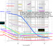
The -v version:
I've spent about a thousand bucks to buy 16 dual JFETs from Interfet
with Mouser as distributor. 8 of those are measured. The plots of Id
versus Vgs show that you cannot even put them in parallel without
presorting because there are Vgs where one is completely open
while another one is completely closed. Thusly gm does not add up,
only the huge capacitances do. Apart of that, the voltage noise
is not so impressive in real life as in the data sheet.
Gerhard
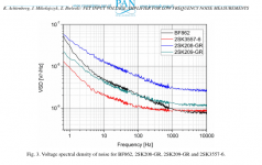
Hi, while I got the message the first time, I much appeciate you clarifying it for the future generations reading this. I understood that the parameters were all over the place as if it still were 1969, while the pricing is worse than 1969.
The voltage noise had always been unimpressive to me. For the die size, it was questionable as to why it isn't loads better.
The BF862 is brilliantly simple in many ways: it uses square drain/source terminals, with n+ nearly as big as the whole drain/source elements. The GATE thus forms a GRID, much like in the TRIODE vacuum valve era.
I believe this is the source of the best photo.
https://zeptobars.com/en/read/BF862-low-noise-N-Channel-JFET-J-FET-AM-preamp-2Ap
There is another one at https://www.richis-lab.de/FET17.htm
For low noise, the W/L ratio of the JFET channel matters a lot. Think of it as a mathematical problem of averaging generated noise. The longer a semiconductor is, the more noise it generates at the same level of defects/etc that generates noise. The wider it is, the more of the generated noise gets averaged out.
And BF862 excels in that manner. The channel length (under the gate/grid) is about 2-micrometers or so. OK, here are my notes: 5643 micrometers channel width, 712 conductive channels in total. Can you imagine? The chip has 5.6 milimeters wide transistor!
Another explanation: apart of the Drain and Source n+ contacts taking most of their area/volume, there is the virtual/real/noise resistance given by gamma/gm
I do not see how to add equations in this, ... ah well, I had to find the source for you! http://dx.doi.org/10.1016/j.nima.2015.08.042
You can see that for low series white noise, we want a low GAMMA, that is when Vgs ~ Vp, which is not what we'd like 🙁, but the Vp = Vds + Vbi, and I find this strange, because this would favor MMBF5103 at -0.98V VGS? But only very slightly, that is. If the gm suffers, there is no point! But you see how knowing ALL the interrelationships is VERY important!
The interesting results are, that SiC JFET has gate leakage thousand billions billions billions times lower than Silicon JFET.
As I lost the ability to speak, here are the equations and pictures, part 1. (P.S. funny to see the channel width parameters can be calculated back from the capacitance change with applied reverse voltage!)
Attachments
-
 Siliconix Noise 1.png66.3 KB · Views: 172
 -
 Siliconix Noise 2.png47.8 KB · Views: 142
 -
 Si SiC JFET Noise 1.png26.1 KB · Views: 147
 -
 Si SiC JFET Noise 2.png30.3 KB · Views: 131
 -
 Si SiC JFET Noise 3 Vbi Ci Ws.png36.2 KB · Views: 129
 -
 Si SiC JFET Noise 4 mat params results.png67.4 KB · Views: 149
 -
 BF862-zoom-HD.jpg418.2 KB · Views: 145
- Home
- Amplifiers
- Solid State
- LTSPICE models of worst-case BF862 JFETs