I've been wanting to design and simulate a few circuits using the BF862 JFET, and I decided I had better use LTSPICE models that I truly believe in. So I measured some transistors myself and fitted the LTSPICE JFET model parameters myself.
I've chosen to take a Worst Case Analysis approach: I measured 100 BF862 transistors, purchased on 3 different dates from 2 different distros (Mouser, DigiKey) and found the two Worst Case devices: the "slowest" BF862, and the "fastest" BF862 in my collection. Then I fitted LTSPICE models to each of these FETs. I figure if my circuit designs work well with the Worst Case transistors, those designs ought to also work well with Typical transistors that fall somewhere between the fastest and the slowest devices I fitted.
(This design approach is called Vertex Analysis when performing design-for-yield optimization; you can read more about it in Spence and Soin's book. It's the approach used to design MOS integrated circuits at Intel, ST Micro, and all of the Silicon Valley startups I ever worked for. Make it work in the worst case: presto it works everywhere else too.)
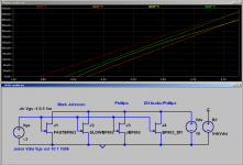
Figure 1 below shows my measurements of the two worst case BF862s I found. The "fastest" (highest current) one is plotted in red; her IDSS is about 21mA. The "slowest" transistor (lowest current) is plotted in blue; her IDSS is about 10mA. NXP's BF862 datasheet says that min_IDSS is 10mA and max_IDSS is 20mA so these measurements are at the outer limits of datasheet approval. Figure 2 shows the LTSPICE simulation results using my fitted models: green for the fastest, red for the slowest. Agreement with measurement (Fig. 1) is pretty good. The simulation circuit is shown in Figure 3.
And here are my fitted model parameter sets:
The goodness-of-fit plots are Figures 4 and 5. I've overlaid the measurement data (dots) with the LTSPICE simulation results (lines). You can see that my curve tracer's channel-2 has a 38mV offset: when I tell it to output -200mV, it actually puts out -162mV. So that's why the VGS numbers at the far right edge of the plot are so goofy-looking. They're offset 38mV from my utterly non goofy steps of 0, -0.1, -0.2, -0.3, -0.4, et cetera. Annoying but not fatal, especially since we're trying to get Worst Case models and not Perfect Fit models.
Figures 6 and 7 show the measured data for the gate-to-source junction diodes. {Remember, these are JFETs with PN diodes, not oxide insulators, on the gate}
If the DIYA posting software lets me, I'm also trying to attach Figures 8-10. These are the simulated I-V curves for the fastest and slowest transistors, plus the simulation circuit. Notice the annoying but nonfatal 38mV offset in the simulation control statement.
Please feel free to use, redistribute, design commercial products with, and/or sell these LTSPICE models. They're completely free with no strings attached. However, at that price, you don't get any technical support either. Here they are; there is no more.
Mark Johnson
I've chosen to take a Worst Case Analysis approach: I measured 100 BF862 transistors, purchased on 3 different dates from 2 different distros (Mouser, DigiKey) and found the two Worst Case devices: the "slowest" BF862, and the "fastest" BF862 in my collection. Then I fitted LTSPICE models to each of these FETs. I figure if my circuit designs work well with the Worst Case transistors, those designs ought to also work well with Typical transistors that fall somewhere between the fastest and the slowest devices I fitted.
(This design approach is called Vertex Analysis when performing design-for-yield optimization; you can read more about it in Spence and Soin's book. It's the approach used to design MOS integrated circuits at Intel, ST Micro, and all of the Silicon Valley startups I ever worked for. Make it work in the worst case: presto it works everywhere else too.)
Figure 1 below shows my measurements of the two worst case BF862s I found. The "fastest" (highest current) one is plotted in red; her IDSS is about 21mA. The "slowest" transistor (lowest current) is plotted in blue; her IDSS is about 10mA. NXP's BF862 datasheet says that min_IDSS is 10mA and max_IDSS is 20mA so these measurements are at the outer limits of datasheet approval. Figure 2 shows the LTSPICE simulation results using my fitted models: green for the fastest, red for the slowest. Agreement with measurement (Fig. 1) is pretty good. The simulation circuit is shown in Figure 3.
And here are my fitted model parameter sets:
Code:
*
.MODEL  FASTBF862  NJF( VTO=-8.238E-1  BETA=2.812E-2  LAMBDA=1.133E-2 IS=6.82E-14   N=1.235
+                       ISR=3P         NR=2           RS=0.5         RD=0.5         BETATCE=-0.5
+                       VTOTC=-2E-3    ALPHA=1E-3     VK=6.0E2       M=0.6          PB=0.5
+                       FC=0.5         CGS=9.5P       CGD=7.5P       KF=8.75E-17    AF=1
+                       MFG=NXP)
*
*
.MODEL  SLOWBF862  NJF( VTO=-5.083E-1  BETA=3.394E-2  LAMBDA=2.426E-2 IS=1.19E-13   N=1.255
+                       ISR=3P         NR=2           RS=0.5         RD=0.5         BETATCE=-0.5
+                       VTOTC=-2E-3    ALPHA=1E-3     VK=6.0E2       M=0.6          PB=0.5
+                       FC=0.5         CGS=9.5P       CGD=7.5P       KF=8.75E-17    AF=1
+                       MFG=NXP)
*
*Figures 6 and 7 show the measured data for the gate-to-source junction diodes. {Remember, these are JFETs with PN diodes, not oxide insulators, on the gate}
If the DIYA posting software lets me, I'm also trying to attach Figures 8-10. These are the simulated I-V curves for the fastest and slowest transistors, plus the simulation circuit. Notice the annoying but nonfatal 38mV offset in the simulation control statement.
Please feel free to use, redistribute, design commercial products with, and/or sell these LTSPICE models. They're completely free with no strings attached. However, at that price, you don't get any technical support either. Here they are; there is no more.
Mark Johnson
Attachments
-
 Figure1.png37.4 KB · Views: 1,233
 -
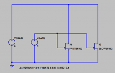 Figure10.png8.8 KB · Views: 481
 -
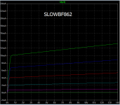 Figure9.png20.4 KB · Views: 427
 -
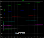 Figure8.png21.9 KB · Views: 405
 -
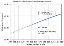 Figure7.png36.2 KB · Views: 521
 -
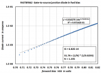 Figure6.png35.1 KB · Views: 566
 -
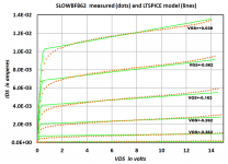 Figure5.png48.8 KB · Views: 1,672
 -
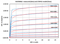 Figure4.png51.8 KB · Views: 1,172
 -
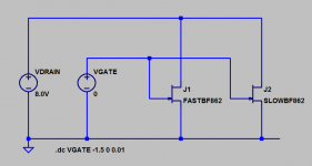 Figure3.png6.9 KB · Views: 1,179
 -
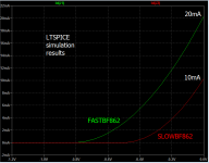 Figure2.png23.9 KB · Views: 1,197

x2--thanks!
Given the population you have, any chance you have an IDSS histogram? (Or raw if you don't feel like going through the trouble of posting the plot)
Given the population you have, any chance you have an IDSS histogram? (Or raw if you don't feel like going through the trouble of posting the plot)
Very useful, thank you!
The parameters I found when fitting the data sheet plots are btn your fast and slow results. So somewhat consistent if that means anything.
Any chance you may fit and publish your median BF862, too? Would be interesting where it falls relative to the extremes.
Are you planning for series production of circuits? B/c in DIY I guess we have the option to discard duds if we know what to look for. I guess your data can help finding what to look for.
Wow! Nice work 
Thank you.
Looks like the BF862 is the "new" go to JFET like how we used to go to the 2SK170?
I use Tina and not Spice, if anyone can give tips how to load a model into Tina, please point me in the right direction.
Thank you.
Looks like the BF862 is the "new" go to JFET like how we used to go to the 2SK170?
I use Tina and not Spice, if anyone can give tips how to load a model into Tina, please point me in the right direction.
Last edited:
Here is a quick comparison. One model is the original model from Phillips. The other seems to be a modification of it.
The square root of the Vgs curves is plotted, and we can see that the Phillips models is a bit more complex than the others. It has a much higher Rs of 7.5R which could be significant for noise.
Simulation models for Jfets are pretty bad as far as curve matching unfortunately.
The square root of the Vgs curves is plotted, and we can see that the Phillips models is a bit more complex than the others. It has a much higher Rs of 7.5R which could be significant for noise.
Simulation models for Jfets are pretty bad as far as curve matching unfortunately.
*
.MODEL FASTBF862 NJF( VTO=-8.238E-1 BETA=2.812E-2 LAMBDA=1.133E-2 IS=6.82E-14 N=1.235
+ ISR=3P NR=2 RS=0.5 RD=0.5 BETATCE=-0.5
+ VTOTC=-2E-3 ALPHA=1E-3 VK=6.0E2 M=0.6 PB=0.5
+ FC=0.5 CGS=9.5P CGD=7.5P KF=8.75E-17 AF=1
+ MFG=NXP)
* by Mark Johnson
*
.MODEL SLOWBF862 NJF( VTO=-5.083E-1 BETA=3.394E-2 LAMBDA=2.426E-2 IS=1.19E-13 N=1.255
+ ISR=3P NR=2 RS=0.5 RD=0.5 BETATCE=-0.5
+ VTOTC=-2E-3 ALPHA=1E-3 VK=6.0E2 M=0.6 PB=0.5
+ FC=0.5 CGS=9.5P CGD=7.5P KF=8.75E-17 AF=1
+ MFG=NXP)
* by Mark Johnson
*
.model JBF862 NJF(Beta=47.800E-3 Betatce=-.5 Rd=.8 Rs=7.5000 Lambda=37.300E-3 Vto=-.57093
+ Vtotc=-2.0000E-3 Is=424.60E-12 Isr=2.995p N=1 Nr=2 Xti=3 Alpha=-1.0000E-3
+ Vk=59.97 Cgd=7.4002E-12 M=.6015 Pb=.5 Fc=.5 Cgs=8.2890E-12 Kf=87.5E-18
+ Af=1)
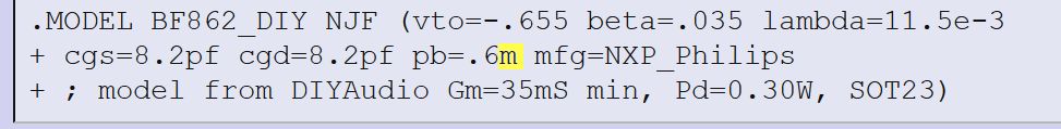
.MODEL BF862_DIY NJF (vto=-.655 beta=.035 lambda=11.5e-3
+ cgs=8.2pf cgd=8.2pf pb=.6m mfg=NXP_Philips
+ ; model from DIYAudio Gm=35mS min, Pd=0.30W, SOT23)
Attachments
I really did look for source resistance but I didn't find any. The linear region IV curves really did appear linear, bearing in mind that my curve tracer isn't the the most precise instrument in the world when operating down at VDS= 150 millivolts.
_
_
Attachments

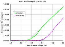
Not sure what those curves are meant to show. Why would you test for Rs at 150mVds? Is the Y scale divided by 10?
Not wanting to nitpick your models, I just want some data to experiment with.
EDIT: So, in the "linear" region of the Jfet which is analogous to the saturation region of a BJT, Rs appears as nonlinearity. That much makes sense. BUT, as the first post charts show, the simulation model doesn't really do linear region. So maybe Rs=7.5 in the Phillips model was meant to work around bad linear region modeling?
Last edited:
I recommend that you repeat the experiment, ideally by purchasing your JFETs from other suppliers to ensure you get different fab-lots than I got.
This won't be terribly expensive:
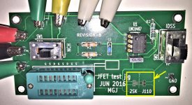
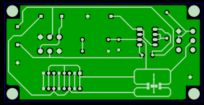
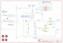
I decided to build a little PCB "jig" to help me measure the BF862s in their native SMD packages -- see yellow box on the photo. Then I took the 5 fastest and the 5 slowest, mounted them on SMD-to-ThruHole adapter boards, and put those on the Curve Tracer. I don't trust the jig's results to any accuracy better than 15% because the contact pressure between JFET and board was not controlled. {A Ticonderoga #2 pencil+eraser pushing the little booger down onto the board @ fingertip pressure}. So I thru-hole mounted the supposedly 5 fastest and supposedly 5 slowest, then chose the Real Winners from thru-hole devices measured on the curve tracer.
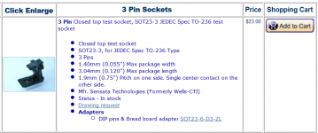
But you are not me, and you may not want to spend the time and money to build a sorting jig. Which is perfectly fine. There do seem to be SOT-23 test sockets for sale on eBay; although I don't have the guts to trust them, myself, perhaps you do.
(By the way, checkout the input bias current spec on that opamp: Cowabunga! Between that and the 100 Megohm bias network, you bet that I wiped that board down with 99% IPA, 6 times after soldering, and once every 2 hours during measurements!)
This won't be terribly expensive:
- 100 BF862s @ $0.27 = $27.00
- 1 curve tracer = $200
- (optional) home made sorting jig as in photos below = $40
- 10 SMD to thru hole adapter boards = $10.00
- 1 copy of Practical Device Modeling (used) = $7.00
- Total = $284
I decided to build a little PCB "jig" to help me measure the BF862s in their native SMD packages -- see yellow box on the photo. Then I took the 5 fastest and the 5 slowest, mounted them on SMD-to-ThruHole adapter boards, and put those on the Curve Tracer. I don't trust the jig's results to any accuracy better than 15% because the contact pressure between JFET and board was not controlled. {A Ticonderoga #2 pencil+eraser pushing the little booger down onto the board @ fingertip pressure}. So I thru-hole mounted the supposedly 5 fastest and supposedly 5 slowest, then chose the Real Winners from thru-hole devices measured on the curve tracer.
But you are not me, and you may not want to spend the time and money to build a sorting jig. Which is perfectly fine. There do seem to be SOT-23 test sockets for sale on eBay; although I don't have the guts to trust them, myself, perhaps you do.
(By the way, checkout the input bias current spec on that opamp: Cowabunga! Between that and the 100 Megohm bias network, you bet that I wiped that board down with 99% IPA, 6 times after soldering, and once every 2 hours during measurements!)
Attachments

How well matched are they generally within batches? I have used some in a prototype amp recently. The first pair had offset under 50mV, could be much lower, I couldn't tell because of a LF noise issue. I switched them with another pair and then after I fixed the problem the output offset is about 5mV.
I repeated keantoken's simulation with the parameters I found when fitting to the charactersitic curves given in the datasheet Fig.8.

The data sheet model falls much closer to the fastBF862 than to the slow one.
The NXP model suffers from the large Rs bending the curve downwards. If it wasn't for that the curve would be much steeper (cf. beta). Heaven knows...
Code:
*
.MODEL  FASTBF862  NJF( VTO=-8.238E-1	BETA=2.812E-2	LAMBDA=1.133E-2	IS=6.82E-14	N=1.235
+                       ISR=3P		NR=2		RS=0.5		RD=0.5		BETATCE=-0.5
+			VTOTC=-2E-3	ALPHA=1E-3	VK=6.0E2	M=0.6		PB=0.5
+			FC=0.5		CGS=9.5P	CGD=7.5P	KF=8.75E-17	AF=1
+			MFG=NXP)
* by Mark Johnson
*
.MODEL  SLOWBF862  NJF(	VTO=-5.083E-1	BETA=3.394E-2	LAMBDA=2.426E-2	IS=1.19E-13	N=1.255
+                       ISR=3P		NR=2		RS=0.5		RD=0.5		BETATCE=-0.5
+			VTOTC=-2E-3	ALPHA=1E-3	VK=6.0E2	M=0.6		PB=0.5
+			FC=0.5		CGS=9.5P	CGD=7.5P	KF=8.75E-17	AF=1
+			MFG=NXP)
* by Mark Johnson
*
.MODEL  JBF862  NJF(	Vto=-.57093	Beta=47.800E-3	Lambda=37.3E-3	Is=424.60E-12	N=1
+                       Isr=2.995p	Nr=2		Rs=7.5		Rd=.8         	Betatce=-.5
+			Vtotc=-2E-3	Alpha=-1E-3	Vk=59.97	M=.6015		Pb=.5
+			Fc=.5		Cgs=8.2890E-12	Cgd=7.4002E-12	Kf=87.5E-18	Af=1
+			Xti=3)
* by NXP
*
.MODEL  dsBF862  NJF(	Vto=-0.763785	Beta=2.592E-2	Lambda=.02244	Is=5.3E-15	N=1.11
+                       Isr=2.995p	Nr=2		Rs=0.5		Rd=.8         	Betatce=-.5
+			Vtotc=-2E-3	Alpha=-1E-3	Vk=59.97	M=.6015		Pb=.5
+			Fc=.5		Cgs=8.2890E-12	Cgd=7.4002E-12	Kf=87.5E-18	Af=1
+			Xti=3)
* NXP model with Is, RS and N from MJ:14Aug2016
* beta, lambda, Vto fit to datasheet Fig.8 by ElFishi
The data sheet model falls much closer to the fastBF862 than to the slow one.
The NXP model suffers from the large Rs bending the curve downwards. If it wasn't for that the curve would be much steeper (cf. beta). Heaven knows...
How well matched are they generally within batches?

My last batch of 16. Two are not shown b/c I killed them probably by testing 🙄.
Not exactly Idss I am measuring, but good enough for sorting.
I don't know because I wasn't looking for that. And, even if I was hoping to quantify matching accuracy, my SMD "test fixture" wasn't sufficiently well controlled to meet a 2% confidence interval. C'mon, a human test operator pressing an SOT23 onto a PCB with a pencil eraser? Really?How well matched are they generally within batches?
That's why I only used the SMD "test fixture" to perform a coarse sieve. Then solder all 10 candidate parts onto SMD-to-thruhole adapter boards and retest them on the higher accuracy curve tracer with known-good ZIF test socket.
To do a creditable job of matching SMD JFETs you will probably have to buy a few different SOT23 test sockets from a few different vendors around the world. Monkey with them, take some measurement data, and find the most reliable / repeatable / trustworthy socket. Then mount two of those side by side on a test DUT board. There seems to be one US vendor (picture below) and several more in China: Ali express link
_
Attachments
The plots of measured I-V versus LTSPICE modeled I-V, suggest to me that if I want my circuit designs to work properly in the worst cases, I had better operate the BF862 with at least 3.5-4.0 volts from drain to source. At any smaller VDS, the SPICE simulation accuracy plummets. I don't want that. For all you JFET cascoders out there, here's a design datapoint.
_
_
Attachments


The plots of measured I-V versus LTSPICE modeled I-V, suggest to me that if I want my circuit designs to work properly in the worst cases, I had better operate the BF862 with at least 3.5-4.0 volts from drain to source. At any smaller VDS, the SPICE simulation accuracy plummets. I don't want that. For all you JFET cascoders out there, here's a design datapoint.
Doesn't make much sense. Saturation onset is at Vds=|Vgs-Vp| and twice this value ensures a good saturation operating point. For devices working around Idss (Vgs=0) this is at 2 pinch voltages, that is not more than 2V (worst case). I've used BF862 at Vds=2.5V without any problem (noise or linearity wise).
Low noise jfets should be run at the lowest possible Vds, since otherwise there's a good chance to degrade the noise performance by hot carrier injection (from the reverse biased gate-drain junction) in the gate.
4V is probably not to bad for the BF862 anyway, but other devices like the 2SK3557 (Vdsmax=15V) are not that happy (noise wise) at Vds=4V, I can tell you that. Also in your post #18, it appears the "fast" DUT you are using as an example has a measured Vp well in excess of 1.2V (around 1.6-1.8V eyes only estimate) which is highly unusual and definitely outside the data sheet (Vp=1.2V max). Strange enough, since high Vp always leads to a lower transconductance (for a fixed device geometry, and barring any short channel effects).
BTW, why do you call those two BF862 classes you are using "slow" and "fast"?
Last edited:
So what are your experiences with the 2SK3557 ?
On datasheet level, it looks almost identical to the BF862.
Thanks,
Patrick
On datasheet level, it looks almost identical to the BF862.
Thanks,
Patrick
- Home
- Amplifiers
- Solid State
- LTSPICE models of worst-case BF862 JFETs