You should make it so AC1/AC1 are AC1 and AC2 that correspond to input 1 and input 2 on the chip.
By the way, do you consider a redesign of the crc board as well ? Could it be made like two twins insteads of one bipolar design ? That way anyonw could use bridges between the twins and have a choice if you use them for bipolar or two mono suplies...
By the way, do you consider a redesign of the crc board as well ? Could it be made like two twins insteads of one bipolar design ? That way anyonw could use bridges between the twins and have a choice if you use them for bipolar or two mono suplies...
Hi Blitz,
It will call for a redesign of PCB .
In the existing PCB itself, one can cut it right down the middle to make it +Ve
or -Ve supply.
regards
prasi
Hi Blitz,
It will call for a redesign of PCB .
In the existing PCB itself, one can cut it right down the middle to make it +Ve
or -Ve supply.
regards
prasi
In continuation to above post....
To Blitz,
I can make a new compact design separately for you with 100mm x 100 mm.
With LT4320 and CRC for single supply. you can get the PCBs produced cheaply at pcbway / jlcpcb.
regards
prasi
For aligning phases.
Aha,
they are actually labelled as AC1 and AC1' .
LT4320 based active rectifier
However, i will label them as AC1 and AC2🙂.
Haven’t all of your previous psu boards consistently used the above notation to aid with transformer phase?
Last edited:
Yes, all of them. I think destroyer read them as AC1 and AC1, which i am guessing.
I did not notice the apostrophe.
Hi Prasi, I am getting ready to stuff some of your original active bridge controller PCB's. I have snubber values for cx,cs and rs and MOSFET's but am stuck on values for C1 and C2.
I've searched this thread but can't find a BOM for the original boards?
I've searched this thread but can't find a BOM for the original boards?
What is the latest PCB/BOM for the CRC PSUs? It looks like the documents for Edit #4 in Post #1 are for the previous design and are no longer up to date?
no , those are the one still produced and sold.
After that , there hasnt been a revision , yet.
After that , there hasnt been a revision , yet.
Last edited:
OK, thanks. I'll poke my head in and check around every now and then for the next GB.no , those are the one still produced and sold.
After that , there hasnt been a revision , yet.
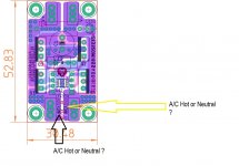
Please clarify hot or neutral phase on pic. Thanks
This is not a mains circuit. You need a transformer ( with dual secondaries) in between with secondary voltage of less than 50VAC. One pair ( 0 and <50 VAC), is connected to the above board to get rectified DC voltage and then further apply smoothing bulk caps to get DC voltage to apply to your amplifier and other circuit.
Just to close the loop on the CT-Discussion...I found this comment from Analog:
"but you could use the LT4320 with both windings out of phase. In this configuration, the center tap would be ground to your load while the LT4320 would have a separate local ground that would the be the "lowest" potential. These nodes are completely separated, with perhaps 10uF of biasing capacitance between them.
IN1 would connect to pin 3 on your transformer, and IN2 would connect to pin 6. The circuit would then use only two MOSFETs to rectify the positive output, these MOSFETs would connect from transformer pins 3 and 6 to OUTP. Then two diodes are connected from OUTN to each input pin to assure OUTN stays low. These diodes will not conduct the load current. The bottom gate pins are unused in this configuration. Finally, the load is connected between OUTP and the center tap."
...not sure how exactly the schematic would look like to be honest...what tyoe of diodes ? just some 1n4007 ?
LT4320 with center tapped Transformer - Q&A - Power By Linear - EngineerZone
Last edited:
- Home
- Group Buys
- LT4320 based active rectifier