Lower chipamp distortion through better PCB routing
I wanted to apply to chipamp design what I learned from Bruno Putzeys' article "The G Word, or How to Get Your Audio off the Ground", originally published in Linear Audio Vol.5. The key learnings for me there were:
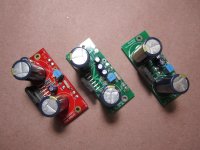
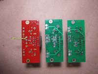
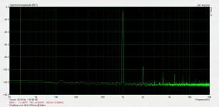
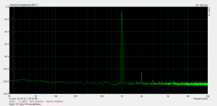
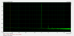
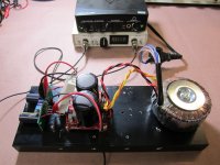
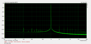
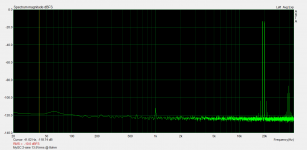
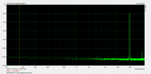
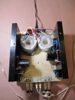
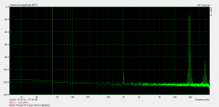
Attached are the spectra of the NOS ChipAmp.com's LM3886 board and two of my boards giving 18V RMS @ 1kHz into 8ohm resistive load. To give you an idea of my measurement setup noise and distortion, I also include the loopback (a.k.a GenMon) performance of my test setup with no amplifier connected (E-MU 0204 sound card with Pete Millett's sound card interface - see the photo of my test bench). The spectra were taken by ARTA software.
Note how a different PCB layout affects the THD performance. Not only the overall THD level is affected, the proportion of higher-order harmonics (which are bad for subjective performance) also changes. Same general layout, same parts, chips form the same batch. Also, note that the distortion and noise of my boards are not that much higher than my measurement floor...
UPDATE: a couple of spectra with a lower noise floor are attached to the post #26 below.
UPDATE2: boards are now available at HiFiOcean.com.
I wanted to apply to chipamp design what I learned from Bruno Putzeys' article "The G Word, or How to Get Your Audio off the Ground", originally published in Linear Audio Vol.5. The key learnings for me there were:
- Each signal has its own reference;
- A single GND pour not a good reference for any signal;
- The signal and its reference should travel together; and
- The signal and its reference should look into balanced impedances.
Attached are the spectra of the NOS ChipAmp.com's LM3886 board and two of my boards giving 18V RMS @ 1kHz into 8ohm resistive load. To give you an idea of my measurement setup noise and distortion, I also include the loopback (a.k.a GenMon) performance of my test setup with no amplifier connected (E-MU 0204 sound card with Pete Millett's sound card interface - see the photo of my test bench). The spectra were taken by ARTA software.
Note how a different PCB layout affects the THD performance. Not only the overall THD level is affected, the proportion of higher-order harmonics (which are bad for subjective performance) also changes. Same general layout, same parts, chips form the same batch. Also, note that the distortion and noise of my boards are not that much higher than my measurement floor...
UPDATE: a couple of spectra with a lower noise floor are attached to the post #26 below.
UPDATE2: boards are now available at HiFiOcean.com.
Attachments
-
 IMG_0701.jpg945.8 KB · Views: 1,521
 -
 IMG_0702.jpg925.5 KB · Views: 1,507
 -
 ChipAmp.com 1kHz 18Vrms @ 8ohm.png59.4 KB · Views: 1,540
 -
 MyGC TH 1kHz 18Vrms @ 8ohm.png60.8 KB · Views: 1,451
 -
 MyGC SMT 0.1% 1kHz 18Vrms @ 8ohm.png61.1 KB · Views: 1,420
 -
 EMU0204+IF 1kHz loopback.png60.7 KB · Views: 671
 -
 IMG_0697.jpg806.6 KB · Views: 772
Last edited:
Just to make sure you've seen this and the accompanying material from TomCHR?
An open source layout for the lm3886 ?
Edit to add in my shortness, excellent work by the way! I meant to say that this complements what has been written/designed/measured as well.
An open source layout for the lm3886 ?
Edit to add in my shortness, excellent work by the way! I meant to say that this complements what has been written/designed/measured as well.
Last edited:
That's pretty damn good. It's great to see more good options for the lm3886. Congrats. 🙂
Looking at your graphs, you're probably held up by your soundcard setup. My thd measurements on a lm3886 at the same voltage give a thd of 0.0013% and a thd+n of 0.0024%. I attach a pic of my amp at the same output (25vp, 50vpp) to give you an idea of what could be hiding under the noise floor. But it's so down under...
Looking at your graphs, you're probably held up by your soundcard setup. My thd measurements on a lm3886 at the same voltage give a thd of 0.0013% and a thd+n of 0.0024%. I attach a pic of my amp at the same output (25vp, 50vpp) to give you an idea of what could be hiding under the noise floor. But it's so down under...
Attachments
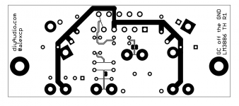
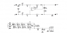
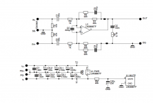
Schematic and BOM - through hole version
As promised, attached are the schematic and the board images.
The BOM is as follows:
As promised, attached are the schematic and the board images.
The BOM is as follows:
- All resistors except RZ - Phoenix SFR16S or similar compact metal film, 1% or better. Vishay CMF50/RN50 would be a good choice.
- RZ - KOA Speer MOSX1 or a similar compact 1W resistor.
- C1, C2 - Panasonic EEU-FC1H152L. Alternatively, the board will accommodate snap-in capacitors up to 22mm in diameter or smaller 100uF 50V capacitors (in which latter case you can also install C3 and C4.
- C3, C4, CZ - Kemet PHE426.
- CI, CF - Panasonic ECE-A1VN220U or similar bi-polar.
- CM - Panasonic EEU-FC1E101S or similar; I used Epcos because I had them.
- U1 - LM3886.
Attachments
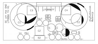

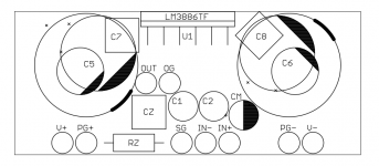
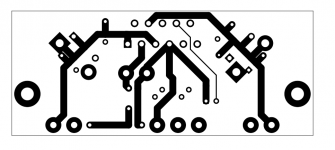
Schematic and BOM - SMT version
Here are the schematic and the board images for the SMT version.
The BOM is as follows:
Here are the schematic and the board images for the SMT version.
The BOM is as follows:
- All resistors except RZ - thin film 0805, 1% or better. I used Susumu RR 0.5% for the test. I did not mount R5 and R6 for the comparison with the ChipAmp.com board.
- RZ - KOA Speer MOSX1 or a similar compact 1W resistor.
- C1, C2 - Panasonic ECE-A1VN220U or similar bi-polar.
- C3, C4, CC - C0G 0805. None of these were mounted for the test.
- C5, C6 - Panasonic EEU-FC1H152L. Alternatively, the board will accommodate snap-in capacitors up to 22mm in diameter or smaller 100uF 50V capacitors (in which case you can also install C3 and C4).
- C7, C8, CZ - Kemet PHE426.
- CM - Panasonic EEU-FC1E101S or similar; I used Epcos because I had them.
- U1 - LM3886.
- R5, R6, C3, C4, and CC are optional. A discussion of them can be found on TomChr's web site; look for the Those Extra “Stability Components” section.
- Unlike the through hole version, this board can be used as inverting, non-inverting, or balanced input amplifier. However, there is a catch: its inverting input must be either driven by a low-impedance source such as an opamp output, or grounded. Floating the inverting input will make this board an oscillator. The reason is that floating the left end of R3 reduces the closed loop gain of LM3886 to less than one, but the chip is designed to be stable when operated at a closed loop gain of 10 or greater. For the test, I connected the inverting input to GND.
Attachments


Thank you DPH and 00940 for quick and positive replies!
I have also seen TomChr's LM3886DR board. Tom has done an admirable job of making his board a solid product, fully documented and characterised.
Thank you - I have seen the thread. My motivation was different, as I wanted to apply to my own design a particular technique that I learned. A chimp amp seemed to be a good application, and I think the results are worth sharing.Just to make sure you've seen this and the accompanying material from TomCHR?
An open source layout for the lm3886 ?
I have also seen TomChr's LM3886DR board. Tom has done an admirable job of making his board a solid product, fully documented and characterised.
I agree - my test setup is noisy and distorting on its own. I may want to run another test with a better oscillator, as my sound card's output seems to be limiting the noise floor more than the input. I would also like to run a test of HF linearity, such as two sine at 19kHz and 20kHz, but for this my current measurement tech is not very revealing.Looking at your graphs, you're probably held up by your soundcard setup.
Having a look at the schematic and layout, it is a bit of a pity that you didn't improve also on the overall design of the amp. Tight PS layout, HF decoupling, output inductor and the like are things that probably won't impact much the 1khz measurements but that could manifest themselves at higher frequencies or in IMD measurements. I understand the desire to compare apple to apple with the chipamp pcb but still...
It would thus be interesting to at least run a pair of other tests even if it pushes the limits of your soundcard (a 10khz test using it at 96khz sample rate).
Further playing the devil's advocate, it might be interesting to actually validate the link between balanced impedance and your results. Unbalance things by using different resistors values for example. My gut feeling is that you're pushing things further than needed with stuff like R6-C4 (smd version).
All good questions.
HF decoupling and an output inductor may help stability, not linearity.
Attached is a 19kHz+20kHz test of the amp. As a baseline, the same test of the soundcard is also attached.It would thus be interesting to at least run a pair of other tests even if it pushes the limits of your soundcard (a 10khz test using it at 96khz sample rate).
My PS layout is tight, provided that the positive and negative supplies are isolated. A bad layout would result in additional non-linearity, as power supply currents would be coupled into the feedback loop.Tight PS layout, HF decoupling, output inductor and the like are things that probably won't impact much the 1khz measurements but that could manifest themselves at higher frequencies or in IMD measurements.
HF decoupling and an output inductor may help stability, not linearity.
R6/C4 allow me to use the SMT version in either non-inverting, inverting or balanced configuration, and the incremental cost is close to nothing in both money and soldering effort. I also think they add to the aesthetics of the design, but that's subjective.My gut feeling is that you're pushing things further than needed with stuff like R6-C4 (smd version).
Attachments
Last edited:
I didn't understand you were using isolated supplies. Your routing makes more sense knowing that. I can't say I'd do it like that for flexibility reasons but it makes sense. 😉
Thanks for the answer.
Thanks for the answer.
To add to grounding techniques it is also important with chip amps to keep the feedback path short or you can get oscillations.
1mm = 1nH of inductance.
1mm = 1nH of inductance.
I use a power supply board from ChipAmp.com, which provides two isolated power supplies. Apologies I have not made this clear up front. I agree a single ground for the two supplies would be another option.I can't say I'd do it like that for flexibility reasons but it makes sense.
Help me understand this one. The typical gain-bandwidth product of LM3886 is 8MHz, according to the datasheet. If my math is correct, the impedance of 1mm = 1nH @ 8MHz would be about 0.05ohms. The typical feedback network around LM3886 would be in 100s Ohm to low kOhm range. In the absence of coupling into the input network, how the additional impedance would affect oscillations? What is the mechanism there?To add to grounding techniques it is also important with chip amps to keep the feedback path short or you can get oscillations.
1mm = 1nH of inductance.
For now, I have a few extra pairs of the actual boards and offer them at the Swap Meet.PCB files are available?
Its not the impedance of the inductor that is important but the phase shift it causes. It can get to the point where the signal is shifted enough in phase to oscillate.Help me understand this one. The typical gain-bandwidth product of LM3886 is 8MHz, according to the datasheet. If my math is correct, the impedance of 1mm = 1nH @ 8MHz would be about 0.05ohms. The typical feedback network around LM3886 would be in 100s Ohm to low kOhm range. In the absence of coupling into the input network, how the additional impedance would affect oscillations? What is the mechanism there?
Let us turn over this stone, too.Its not the impedance of the inductor that is important but the phase shift it causes.
The phase margin of LM3886 is about 65 degrees (see TomChr's site for more data).
The phase shift in an RL network is Phi = atan(X(L)/R), where atan() is the reciprocal of tangent, X(L) = w*L, w=2*pi*Frequency. If X(L) is 0.05ohm @ 8MHz as calculated above, and if R is, say, 1kOhm, the phi = 0.003 degrees.
Should we have a 25mm trace with inductance of 25nH, the phase shift would be 0.07 degrees. Can it really affect stability?
Let us turn over this stone, too.
The phase margin of LM3886 is about 65 degrees (see TomChr's site for more data).
The phase shift in an RL network is Phi = atan(X(L)/R), where atan() is the reciprocal of tangent, X(L) = w*L, w=2*pi*Frequency. If X(L) is 0.05ohm @ 8MHz as calculated above, and if R is, say, 1kOhm, the phi = 0.003 degrees.
Should we have a 25mm trace with inductance of 25nH, the phase shift would be 0.07 degrees. Can it really affect stability?
Its not as simple as that.
To work out phase shift you need to take into account the feedback resistor too. With 25nH and 22K feedback resistor you get 7 degrees phase shift.
25 mm isn't much and if you are up higher then you can quickly get into trouble.
Test mule, now in stereo
Just finished building a minimalistic stereo version - see photos. The test mule looks a bit rough, but my first listening impressions are quite positive.
The test system consists of an exposure 2010S CD player with Tentlabs XO3 low jitter clock upgrade, a NAD M51 DAC/digital preamp, and a pair of full range Fostex speakers in BK-12 backloaded horns. The reference amplifier is BBA3 with zero global feedback.
Attachments


How did you arrive at 7 degrees? In my book, increasing R in an RL circuit increases the pole (aka cutoff, corner, -3dB) frequency and reduces phase shift at low frequencies. If R=22kOhm and L=1uH (I agree 25nH isn't much), the pole frequency is 3.5GHz, and phase shift at 8MHz is about 0.13 degrees. Do I miss something here?Its not as simple as that.
To work out phase shift you need to take into account the feedback resistor too. With 25nH and 22K feedback resistor you get 7 degrees phase shift.
25 mm isn't much and if you are up higher then you can quickly get into trouble.
Details aside, I believe that if long traces are bad, there must be another reason for it, not the inductance.
It's hard to disagree. tomchr showed one way to build good decoupling, and there are other ways. It would be interesting to look into the details of how decoupling (or lack thereof) affects an opamp - it may be obvious for tomchr but not for me.Without good decoupling LM3886 can oscilate with hard loads.
I presume you read tomchr's text.
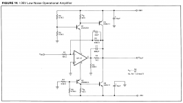
By the way, I know at least one opamp circuit that works happily into a hard load without decoupling - see, for example, the attached schematic. I copied this from Analog Devices' Application Note AN-106, but the circuit itself dates back to older National Semiconductor application notes and is quite popular, including in audio and in this forum. I figure the power supply rail impedance for the opamp is about 20ohm on each rail (assuming h21 of Q1 and Q2 is about 100), much more than any reasonable capacitor would provide.
Attachments
Last edited:
H Do I miss something here?
A capacitive load? Inductance in the feedback network is only an problem as load capacitance goes up. See Tom's page you linked. Hence the need for an output inductor, that reduces the problem significantly.
A capacitive load? Inductance in the feedback network is only an problem as load capacitance goes up. See Tom's page you linked. Hence the need for an output inductor, that reduces the problem significantly.
Thank you - this is very helpful! I can see now that the (low) trace inductance is important when it is in series with the low Zout of the amplifier, not with the relatively high resistance feedback network. That is, the important trace that must be kept short and fat for low inductance is the one between the output pin of LM3886 and the Zobel network.
BTW, there are two other problems with long traces, both addressed with some success in my boards. First, the ohmic resistance of a longer trace, in particular a high current trace such as power ground, amplifier output or power supply, will develop a larger voltage drop along the trace. Ground loops are part of this, but the problem is broader. The other one is that longer traces may facilitate inductive coupling with other traces. Both effects may affect stability and linearity if the voltage drop or inductive coupled voltage adds to the input or feedback signal.
As an illustration, I connected PG+ and PG- on my power supply, and connected power to my board with three wires (V+, V-, PG), not four (V+, PG+, V-, PG-) as before. This made the power supply current loop around the board and couple with various signal traces. The results are attached; you can see that the distortion performance degraded but still is better that that of the ChipAmp.com board.
The output inductor, by the way, did not fit on my small board. One can always connect it between the board and the output binding posts. In fact, the inductance of just a 10-15cm wire may be sufficient - there are competently designed commercial amplifiers, e.g. early Creek models, that use just that.
Attachments

- Status
- Not open for further replies.
- Home
- Amplifiers
- Chip Amps
- Lower chipamp distortion through PCB routing