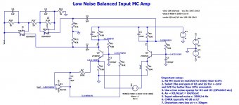
Here's a simple circuit I've been playing with for a balanced input MC pre. I'll do a bit more work on it in the coming few weeks. Its a pretty low cost approach - the most expensive item being a decent dual opamp like the OPA1642 for example. The noise will improve with higher collector currents, but a practical limit would be about 6-8 mA per side - any higher than this and the 5-8V reg will probably need a series pass device.
Note carefully the comments about resistor matching for R1-R4 - the CMRR depends on it!
U1 servos out any DC voltage difference across the emitters of Q1 and Q2 to ensure DC current through the cartridge is minimized. In practice, an OPA2188/9 would be used for this function (I just used the AD745 because this is what was in the LTspice library) as I have done in the X-Altra MC/MM RIAA (that is an unbalanced input, but lower noise). The other half of the servo can be used for the 5-8V reg - the PSRR of these devices is superb, so they work well in low noise servo and low noise regulator functions.
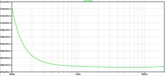
Update 02 January 2022 - I have added the PRELIMINARY 1st cut measurements - see PDF file below
Note carefully the comments about resistor matching for R1-R4 - the CMRR depends on it!
U1 servos out any DC voltage difference across the emitters of Q1 and Q2 to ensure DC current through the cartridge is minimized. In practice, an OPA2188/9 would be used for this function (I just used the AD745 because this is what was in the LTspice library) as I have done in the X-Altra MC/MM RIAA (that is an unbalanced input, but lower noise). The other half of the servo can be used for the 5-8V reg - the PSRR of these devices is superb, so they work well in low noise servo and low noise regulator functions.
Update 02 January 2022 - I have added the PRELIMINARY 1st cut measurements - see PDF file below
Attachments
Last edited:
Its not 47k input - its a current input so about 3 Ohms in this design at c. 3mA collector current and about half that at 8mA per side.
Ah yes. needed to turn your diagram on it's side to make sense. Damned computers never understand the input should be on the left 😀
I don’t understand how the Servo works.
It stabilizes the operating point of Q1, but Q2 can still drift.
Or am I missing something?
It stabilizes the operating point of Q1, but Q2 can still drift.
Or am I missing something?
The servo measures the emitter voltage of Q2 (Vref) and then adjusts the base of Q1 so that the emitter voltage of Q1=Q2. The absolute voltage is not important - only that the voltages are equal so that no DC current flows in the cartridge.
Ah yes. needed to turn your diagram on it's side to make sense. Damned computers never understand the input should be on the left 😀
😀
I originally had it the wrong way around and wondered why LTspice kept grinding to a halt after a few nana seconds 🙂
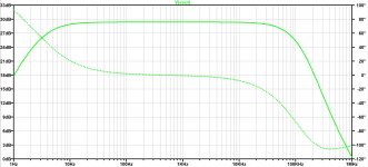
Here's the AC response. If you're pathological about the bass end, the 1uF output caps would need to go to 2.2uF and the 47k resistors to 100k. There is no noise penalty since the Zsource for the differential stage is not more than a few hundred Ohms if you are using a high resistance cart and the collector load resistors go to 300-500 Ohms.
Attachments
I like the look of this. So gain is R3/Rcart, so 10x for a 10 Ohm cartridge, less for a cart with higher resistance. You mention different idle currents, how do you adjust that? Do you need to change all of R1-R4 to adjust the idle current or the gain? Does PS voltage matter gain and idle current? How much current can you push through those Zetex semis without heat sinks, and will sinks allow one to use higher current?
Sorry for the silly questions but this is an unusual (to me) circuit and I do not understand it.
Sorry for the silly questions but this is an unusual (to me) circuit and I do not understand it.
The Zetex transistors can handle 1W dissipation and up to 5A collector currents - they are essential small power transistors! As such they have an exceptionally low base spreading resistance Rbb which is one of the most important parameters for amplifier input stages for low impedance sources. They were never designed as low noise audio parts and the datasheet doesn't mention Rbb or any noise specs.
Here, they are used in a common base configuration (base is grounded, input signal applied to the emitter) providing a very low input impedance (approx 25mV/Ic). In such a circuit topology, they form a current input amp for the MC cartridge.
Here, they are used in a common base configuration (base is grounded, input signal applied to the emitter) providing a very low input impedance (approx 25mV/Ic). In such a circuit topology, they form a current input amp for the MC cartridge.
I don't understand the balancing circuit U2/U3. U2 has a gain of 2 for the voltage on R9 (let's call its input U, output 2U). U3 just inverts this signal (output -2U) and adds the voltage on R11 (let's call it -U) with a gain of -1 (output U). The net output on U3 will be -2U+U= -U.
Why didn't you use a balancer like on a) or b) in this link?
Amplifiers with balanced Inputs or Outputs-TINA and TINACloud
Or just the second half of picture b) without the input buffers.
Why didn't you use a balancer like on a) or b) in this link?
Amplifiers with balanced Inputs or Outputs-TINA and TINACloud
Or just the second half of picture b) without the input buffers.
Its not 47k input - its a current input so about 3 Ohms in this design at c. 3mA collector current and about half that at 8mA per side.
Hi Bonsai,
Nice design for a transimpedance amp without feedback, but a few comments:
With 100R collector resistors and 1.8V on them, Ic=18mA.
Total input resistance is 2*Rbb +2*(1/2Gm) = 2*1.5 + 2*(1/1.44) = 4.4R
This 4.4R will produce 0.27nV/rtHz, very close to what you specified.
With a 1R Cart, gain is indeed 100/1 = 100.
But taking a 10R Cart, gain is not 100/10=10 but 30.
Hans
Because the 3 nV is referred to the output of the input stage and not it’s input. At that point, the signal is about 5 mV.
Vnoise is always given ref input of opamp, how can opamp datasheet know what gain we use? I sim your circuit and get 42nV/rtHz, which makes NO sense since I get gain ca 37dB, so I am still confused b/c noise should be more like 60x3nV=180nV/rtHz.
Obviously I don't quite get it yet...
Obviously I don't quite get it yet...
The amp consists of two stages - the input stage with discrete transistors and the opamp summing and output stage. If you have two stages in series, the overall noise basically is calculated as (input stage noise) + (output stage noise / gain of input stage). If the input stage has significant gain (which is the case in this amp), noise of the second stage does not contributes much to the overall noise !
Remember the gain is proportional to the resistance of the cart. So for noise, set the generator resistance to 0.1 Ohm then this will give you the input referred noise of the total circuit only. Then to check gain, put the cart residence in. I used 10 Ohms (typical MC cart) and also 30 ohms ( DL103 is about 30 Ohms).
Note that the gain with the cart set to 0.1 ohm will be very high, but the noise sim takes care of this and still calculated the correct input referred noise.
Note that the gain with the cart set to 0.1 ohm will be very high, but the noise sim takes care of this and still calculated the correct input referred noise.
- Home
- Source & Line
- Analogue Source
- Low noise Balanced MC Pre