Hi,
is that Baxandall's diode in the output stage?
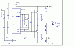
There are some other components required to get the handover to work better in a quasi output stage. Find JohnL Hood's version.
I think the diode is in the wrong place.
is that Baxandall's diode in the output stage?
There are some other components required to get the handover to work better in a quasi output stage. Find JohnL Hood's version.
I think the diode is in the wrong place.
his book shows
D=1s820?
R=100r
C=20nF
I guess these are to mimic the characteristics of the BE junction of Q3 and may take quite a bit of experimentation.
Crimson used something similar.
D=1s820?
R=100r
C=20nF
I guess these are to mimic the characteristics of the BE junction of Q3 and may take quite a bit of experimentation.
Crimson used something similar.
the resistor // to the diode seems to be the mirror of the driver's emitter one in most of schematics from the seventies.
I knew this topology before building these amps but i choosed to simplify and to modify later if necessary. The result was i got very clear trebles.
As my ear is satisfied and as i have no possibility to measure distortion, i left the amp unmodified till now.
But i keep on being interested on this Baxandall point.
Lazy cat,
Thank you for your design. Is this original idea from you? Never seen before such a topology. Very clever. I'll try it one day.
Thank you for your design. Is this original idea from you? Never seen before such a topology. Very clever. I'll try it one day.
Anyone contemplating building a design with the LME49810, 49811, 4702 should read this thread:
http://www.diyaudio.com/forums/showthread.php?s=&threadid=132471&highlight=
there's a tweak in the compensation suggested by Bob Pease.
http://www.diyaudio.com/forums/showthread.php?s=&threadid=132471&highlight=
there's a tweak in the compensation suggested by Bob Pease.
Anyone contemplating building a design with the LME49810, 49811, 4702 should read this thread:
I believe this two pole compensation is briefly mentioned in AN- 1850 (LME49830) on page 13.
Just a short quote: from the AN:
"The two-pole compensation scheme allows for increased
loop gain at higher frequencies, resulting in increased slew
rate, dynamics and reduced high-frequency distortion."
I have incorporated the additional R and C in my revised PCB, and will test it in a few days.
What was mentionned is not a two pole compensation.
Here it seems that ( not for the 49810 ??) a serie resistor + capacitor should be added from comp pin to ground while leaving the mille cap in place.
The twin pole compensation is a feedback compensation method replacing the mille capacitor by twin T ( 2 cap and a resistor in the middle). The objective of such a network is to keep constant the loopgain in the midband then decrease it at 40 db/decade and then before the phase margin is too low, come back to 20db/decade to have enough phase margin at unity gain. This method buys you loop gain in the middband. It is of course a tricky method that must be tuned for a topology, a specific load and a layout.
What is mentioned in the thread is more a lag serie compensation added to the loop gain already compensated by the miller feedback compensation. The lag compensation technique decreases the loop transmission in the vicinity of unity gain while not modifying to much the phase margin, therefore it will improve the stability if there are problems with some parasitic poles in the vicinity of the unit loopgain frequency.
JPV
anyone here tested with VERTICAL irfp240 mosfets ?
irfp240 is included in national stereo version IC PDF , and has low THD, good behaviour
So did anyone here try to make irfp version of amplifier and did some tests, I presume 60mA current should be enough to drive 300W mosfet output stage ?
if 5mA can drive single stage thats 10 times more .
irfp240 is included in national stereo version IC PDF , and has low THD, good behaviour
So did anyone here try to make irfp version of amplifier and did some tests, I presume 60mA current should be enough to drive 300W mosfet output stage ?
if 5mA can drive single stage thats 10 times more .
grizlimedo said:anyone here tested with VERTICAL irfp240 mosfets ?
irfp240 is included in national stereo version IC PDF , and has low THD, good behaviour
So did anyone here try to make irfp version of amplifier and did some tests, I presume 60mA current should be enough to drive 300W mosfet output stage ?
if 5mA can drive single stage thats 10 times more .
They really designed the LME49830 for these devices in mind. The LM4702/LME49811 will drive the lateral MOSFETs with no problems.
You might want to consider the Fairchild FQA12P20 and FQA19N20 devices -- a bit less expensive than the Vishay/IRF.
Qoute:" What was mentionned is not a two pole compensation.
Here it seems that ( not for the 49810 ??) a serie resistor + capacitor should be added from comp pin to ground while leaving the mille cap in place"
But that is exactly what is described in AN-1850, page 13?
I agree that Two-pole compensation is the commonly used term for what you describe, but National uses the term Two-pole to describe the compensation scheme in the application note.
Or am I still completely in the mist?😕
jackinnj is right (and so was i..), it is mentioned in AN-1850. They suggest 20pF for Cc, and 5k1/12pF for R1/C1 as drawn in http://www.diyaudio.com/forums/showthread.php?postid=1740575#post1740575:)
Segran said:Qoute:" What was mentionned is not a two pole compensation.
Here it seems that ( not for the 49810 ??) a serie resistor + capacitor should be added from comp pin to ground while leaving the mille cap in place"
But that is exactly what is described in AN-1850, page 13?
I agree that Two-pole compensation is the commonly used term for what you describe, but National uses the term Two-pole to describe the compensation scheme in the application note.
Or am I still completely in the mist?😕
What is shown on page 13 is Two-Pole or Twin pole compensation as I described (with Rc2 removed)
What is mentionned in Jackinnj post is another compensation combining Miller and an equivalent of lead/lag.
JPV
i speak about the lag compensation. Audioman said too: " It is mandatory for that 75pf and 3.3k resistor to be there!!! You will have osc problems coming out of clipping if it is not there."
- Home
- Amplifiers
- Chip Amps
- LME49810 - a new cousin for LM4702