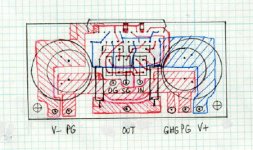
Here's my revised version, which takes care of previous input. The 1K resistors are all Caddocks (or Vishays) and Rikens can be used for gain setting as well in vertical position. All connections and sizes are proper size. The grounding is more symetrical (output ground is taken from a midway point now), signal routing simplified, 2 cap sizes available, mute resistors are SMD.
Attachments
bigparsnip: Your's looks much better than mine. ;-)
Dimensions for the Pansonic FC 50V 1000uF
Digikey: P10333-ND 16mm diameter with 5mm lead pitch.
Digikey P11263-ND 12.5mm diameter with 5mm lead pitch.
I've always used the Dale/Vishay RN series resistors because they are available in a wide range of values/ levels of precision, very low temp coefficient and low noise in general. They are also inexpensive and offered in a standard 1/2W & 1/4W leaded size. Mouser stocks them here in the USA and they are great to deal with.
http://www.vishay.com/docs/31027/cmfmil.pdf
For the output resistors I'd consider the Link Metal Oxide parts from Solen, or Mills.
If you want help on the .lib files let me know. I'd be happy to work on those for you.
Hi, I have gotten the mills 5W ones in there at the minute, and I was probably going to either go for the same caddock riken combination as the LM3875 board unless I hear anything from someone stating that these wouldn't be suitable. (these should slo help shrink the board down a bit as well, as the caddocks have quite a small footprint)
Also, I have change the caps I placed on the board before (no you will be able to use anything from a 5mm pitch up to 10mm pitch at 22.5mm in diameter, the same as the original boards), and along with a few minor tweaks, the board is now down to just 3 by 1.4 inches (and should be just the same size as the original once I have the caddock resistors in there, especialy if I go for all caddock rather than the riken ones).
Also, I have change the caps I placed on the board before (no you will be able to use anything from a 5mm pitch up to 10mm pitch at 22.5mm in diameter, the same as the original boards), and along with a few minor tweaks, the board is now down to just 3 by 1.4 inches (and should be just the same size as the original once I have the caddock resistors in there, especialy if I go for all caddock rather than the riken ones).
Go for it.... everyone seems happy with the Caddock/Riken combo on the 3875.
We need some input from those interested in the group buy. Is this something that everyone would prefer over the National board?
We need some input from those interested in the group buy. Is this something that everyone would prefer over the National board?
Layout of ground(s)
ALW and Peranders are right!!!!
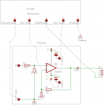
In the attached schematic, imagine 5 amps of current returning through the speaker. This creates a voltage drop across the ground which I've simplified for discussion but it's realistic. Note how the current flows from the speaker ground return pad across the ground plane then underneath the signal ground point and then finally to power supply ground. The sheet resistance of copper is assumed to be 0.45mohm/square. In this example, the signal ground will be elevated by 22.5mv. This then is multiplied by 30 at the output as nearly the full 22.5mv is fed into the negative terminal. So the output voltage (DC case) drops by 30 x 22.5mv ~ 0.7V. That's a lot of distortion if you think about the real waveforms.
My conclusion is that V+gnd, V-gnd and Speaker gnd pads must be virtually on top of each other. Also, the wiring should be directly soldered to the copper and not to a through-hole via on the other side. It's that simple.
-Robert
ALW and Peranders are right!!!!
In the attached schematic, imagine 5 amps of current returning through the speaker. This creates a voltage drop across the ground which I've simplified for discussion but it's realistic. Note how the current flows from the speaker ground return pad across the ground plane then underneath the signal ground point and then finally to power supply ground. The sheet resistance of copper is assumed to be 0.45mohm/square. In this example, the signal ground will be elevated by 22.5mv. This then is multiplied by 30 at the output as nearly the full 22.5mv is fed into the negative terminal. So the output voltage (DC case) drops by 30 x 22.5mv ~ 0.7V. That's a lot of distortion if you think about the real waveforms.
My conclusion is that V+gnd, V-gnd and Speaker gnd pads must be virtually on top of each other. Also, the wiring should be directly soldered to the copper and not to a through-hole via on the other side. It's that simple.
-Robert
Attachments
Robert you don't have to "scared" using pcb. The only thing you have to think about is that you don't add "error" currents. The most important thing is not to let high currents flow in the signal ground. It's also important to keep away current from the smoothing caps from the signal ground.
Even better
Peranders,
No fear here! Was just trying to make a concrete recommendation. I have observed that most recommendations are too vague. Using real values and figuring out real errors is what I like.
Even better than putting all the power ground pads next together would be to common them all at the PS board and send only one large ground wire to the amp board. So that's just one pad for external ground. Note this means the common wire from the speakers must be terminated at the PS and not the amp. Doing it all this way avoids all power related ground currents except the obvious 1000uF capacitor returns flowing in the amp board. This is better, right?
-Robert
My final offer, er, recommendation
One more improvement to grounding.
If there is just one pad to external ground, as I proposed in last post, then there is a problem of resistance between the 2 capacitor ground pads and the main ground pad from the external PS board.
A 12 gauge wire 4" long has a resistance of 0.02 ohm. If the V+ cap and the V- cap are separately connected directly to the PS board ground via 2 such wires, then the maximum ground noise at the amp inputs would now be ~0.2mv, assuming there's another 0.02 ohms connecting the wire through a solder pad then through half a square of copper to the capacitor lead.
Hope this is making sense.
-Robert
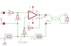
p.s. - Added schematic to help the explanation.
One more improvement to grounding.
If there is just one pad to external ground, as I proposed in last post, then there is a problem of resistance between the 2 capacitor ground pads and the main ground pad from the external PS board.
A 12 gauge wire 4" long has a resistance of 0.02 ohm. If the V+ cap and the V- cap are separately connected directly to the PS board ground via 2 such wires, then the maximum ground noise at the amp inputs would now be ~0.2mv, assuming there's another 0.02 ohms connecting the wire through a solder pad then through half a square of copper to the capacitor lead.
Hope this is making sense.
-Robert
p.s. - Added schematic to help the explanation.
Attachments
for ALW,RFScheer,Peter🙂
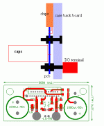
We discuss the layout of pcb, it is not isolated. Should have been at the case, and the peripheral device,and I/O terminal is included too.
all trace(pcb copper,and hock wire)Connect in parallel and meet in 0v ground point.I think have two choices of the place,one set up on the case ground at 0v point,One is a ground that sets up on pcb.
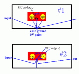
this is a example pic,sorry for my ugly drawing
We discuss the layout of pcb, it is not isolated. Should have been at the case, and the peripheral device,and I/O terminal is included too.
all trace(pcb copper,and hock wire)Connect in parallel and meet in 0v ground point.I think have two choices of the place,one set up on the case ground at 0v point,One is a ground that sets up on pcb.
this is a example pic,sorry for my ugly drawing
Attachments
Digi please amplify
Digi maybe you and I are driving everyone away from this thread, but just in case they are interested, your drawings don't make sense to me.
2 posts up in the thread you propose 2 ground schemes. Input and output are really input_ground and output_ground, right? You're proposing the ground of the rca jack goes to the star point directly I think. Hmmm. I'll think about that. It is often recommended that the input interconnect shield is connected to ground only at the source and is interrupted at the rca jack. This breaks a very bad ground loop that often occurs between equipment.
I like #2 not #1.
I think the natural star point inside the amp is the ps pcb. A copper bussbar mounted to the front of the ps pcb might be ideal.
Regarding the last post, I'm not sure what you're proposing, but let me guess. Is the I/O terminal an rca jack for example that is interfaced directly to the pcb? Same with speaker jacks? Anyway, I like the idea of short, small, directly interfaced jacks. This is like a plate amp configuration but very compact. If the power supply board is piggy-backed same style, then you have a panel with the amp attached and just attach the transformer, power cord, power entry and you're done.
-Robert
sure, RFScheer.
I mean this.I agree in the way of #2 too.If us minimize # 2, as possible as compact...
I post a new thread to discuss this way:
http://diyaudio.com/forums/showthread.php?s=&threadid=33098
please😉
-digi
I mean this.I agree in the way of #2 too.If us minimize # 2, as possible as compact...
I post a new thread to discuss this way:
http://diyaudio.com/forums/showthread.php?s=&threadid=33098
please😉
-digi
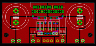
Hi, I have been having a bit more play about with the board layout today, and I have got it so that it will now accept the mills MBR5 resistors for the output, and Caddock MK132 everywhere else (I can't find anywhere that sells the Riken resistors, so I figured it wouldn't hurt just to replace them with the same Value caddocks). I have also put some jumper points on the board so that it can be used either as two seperate chanels (or bridged, with the right inputs), or as on parallel with only one input and output leed.
One thing I was wondering though, is would people mind if the the NC pins had to be removed to place the chip in the board? As I think doing this will make for much neater layout of the tracks and bigger traces for the power and ground to the chip.
One thing I was wondering though, is would people mind if the the NC pins had to be removed to place the chip in the board? As I think doing this will make for much neater layout of the tracks and bigger traces for the power and ground to the chip.
Attachments
I wouldn't have any problem with snipping them. A four-layer board would be cool too and probably worth the extra expense. It would alleviate the need for trimming of the NC pins.
Oh.... buss bar on the PS PCB would get my vote. Have plenty of room to tie all the grounds to one place and one connection to the chassis.
Kevin Haskins said:I wouldn't have any problem with snipping them. A four-layer board would be cool too and probably worth the extra expense. It would alleviate the need for trimming of the NC pins.
I would highly recommend against snipping the NC pins off, as it creates problems. A good solution is to make the copper for the NC pins small, or remove it, and just leave a hole in the PCB, to allow for the traces to be routed easier. Also, round pads might work better then the oval pads, since you will need to route traces through the middle.
4 layer pcbs greatly increase the cost of manufacture and prototyping, so they probably aren't worth it for such a simple design.
--
Brian
Kevin Haskins said:Oh.... buss bar on the PS PCB would get my vote. Have plenty of room to tie all the grounds to one place and one connection to the chassis.
Like the bus bars on the Rowland concentra amp?
--
Brian
Attachments

bigparsnip said:
One thing I was wondering though, is would people mind if the the NC pins had to be removed to place the chip in the board? As I think doing this will make for much neater layout of the tracks and bigger traces for the power and ground to the chip.
While I wouldn't mind clipping the leads off an LM3875 or 3886, the 4780 seems to me to just have too many (and too small) pins for me to be certain I'm removing the right ones, or don't accidently break off an important pin next to one of the NC pins. This may just be from not being able to judge the size well from the pictures, and I may be in the minority, but I'd make every effort to leave them attached. I would recommend you do what Brian did with pin 9 on the LM3875 boards. and just make a hole with no solder pad. That way you have much more room to route traces, without needing to worry about removing the wrong pin.
Actually, when you look at National's evaluation board, those pins are not really in a way and removing them will not simplify trace routing. Those pins are connected either to ground or negative rail. I don't see any advantage in clipping them off and while doing that a mistake could be made, that is not repearable😉
I see resistor pads more disturbing in running PS traces than those pins..
I see resistor pads more disturbing in running PS traces than those pins..
- Status
- Not open for further replies.
- Home
- Amplifiers
- Chip Amps
- LM4780 pcb layout and others