Grounding difference with National
Bigparsnip,
I originally wrote this note with a misunderstanding of your layout so I've edited it somewhat. It's hard to tell but it appears there is a small ground trace in blue for the signal and feedback resistors. How do you connect a wire to this? That's my main concern. And do you intend it to be isolated on the pcb from the main power ground plane? (It must not share a ground trace on the amp pcb with the power supply return paths.)
I think you should place an inboard pad for each capacitor ground very near the capacitor and totally eliminate that large common ground plane. It's of no use.
Has everyone noticed how the National layout isolates the signal star ground from the rest of the pcb and connects it to the shields of the 2 inputs and that's the only connection to a system ground for the signal path.
-Robert
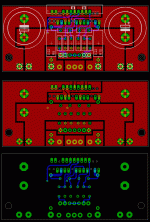
Ok, I've attached a picture of the board as it stands now, with everything wired up (including the mutting resistors, which are rather tiny 0805 parts to make them fit). It basicaly folows the same layout as Brian's original board for the power rails and ground scheem (so there shouldn't be any problems with ground loops) although I have yet to join the signal ground to the power ground on the board as it is on the original, as I wasn't sure if people would want to connect them on the board or off at the main star ground point.
But, if people have any sujestions or ideas, I guess you may as well let me know now (even though I probably won't get much more of a chance to work on it now untill the rest of my exams are over next weekend) and I can think about any modifications I may make.
But, if people have any sujestions or ideas, I guess you may as well let me know now (even though I probably won't get much more of a chance to work on it now untill the rest of my exams are over next weekend) and I can think about any modifications I may make.
Attachments
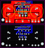
Here is my version that I started on last night based on Peter's sketch, and the National layout. I haven't finished it yet.
Any comments?
(besides the current lack of heat relief traces)
I will probably make the board 0.05-0.1" deeper, and pull the input pads down, allowing for the creation of a wider gnd trace between the input pads and the output pad.
--
Brian
Any comments?
(besides the current lack of heat relief traces)
I will probably make the board 0.05-0.1" deeper, and pull the input pads down, allowing for the creation of a wider gnd trace between the input pads and the output pad.
--
Brian
Attachments
Looks great, Brian. I agree about pushing back the pads for 16 and 18 for a little more room in there. Would putting the wiring connection pads at a 5mm spacing to support terminal blocks be worth while? Triple for input, doubles for the power, and single for the out and ground (poss a triple to include the chassis ground and +power). They look clean and make any component experimentation much easier. Per uses them often and the pics of his designs look very professional with them. I won't comment on any sonic impact they would make, but people could have a choice.
Philo said:Looks great, Brian. I agree about pushing back the pads for 16 and 18 for a little more room in there. Would putting the wiring connection pads at a 5mm spacing to support terminal blocks be worth while? Triple for input, doubles for the power, and single for the out and ground (poss a triple to include the chassis ground and +power). They look clean and make any component experimentation much easier. Per uses them often and the pics of his designs look very professional with them. I won't comment on any sonic impact they would make, but people could have a choice.
The spacing of the pads is 200mil, which is roughly equivilant to 5mm, allowing you to use terminal blocks. You will find that some people used terminal blocks for my LM3875 boards, such as shown here:
http://www.diyaudio.com/forums/showthread.php?postid=381707#post381707
--
Brian
# of caps
Not to be critical of the good work, but there are 2 amps on this chip, shouldn't there be spots for 4 caps?
Not to be critical of the good work, but there are 2 amps on this chip, shouldn't there be spots for 4 caps?
Hey Brian,
So what do you think of the 4780 so far?
Are you going to do a parallel PCB for these or are you still considering one for the 3875?
I still haven't done anything with my 3785 PCB's yet 🙁 Waiting to see what I want to do......
BTW, I just got your email as I haven't been checking things lately. I was preoccupied by trying to pass my final so I can GRADUATE!!! 😀 😀 😀
Re: # of caps
National is using only 2 caps on their evaluation board.
lgreen said:Not to be critical of the good work, but there are 2 amps on this chip, shouldn't there be spots for 4 caps?
National is using only 2 caps on their evaluation board.
Brian,good protel design.I like the traces to be routed smooth🙂
how do you do with protel?
-digi
how do you do with protel?
-digi
cdoggy81 said:Hey Brian,
So what do you think of the 4780 so far?
Are you going to do a parallel PCB for these or are you still considering one for the 3875?
I still haven't done anything with my 3785 PCB's yet 🙁 Waiting to see what I want to do......
BTW, I just got your email as I haven't been checking things lately. I was preoccupied by trying to pass my final so I can GRADUATE!!! 😀 😀 😀
I haven't tried the LM4780 yet. I bought 6 of them from digikey a while back, thinking that I might do something with them, but I have been too busy with a many other things. I just made the layout last night since I was curious with the idea. It wasn't too difficult, given the National Eval board layout, and Peter's drawing up above.
I have all the components for the Bridgeclone ready to go, and even matched resistors set aside, but I just haven't made it into lab yet. I am trying to, but stuff just keeps on coming up.
Congratulations on your graduation! I hope your final goes well. I was so relieved when I finished last semester (I had 2 of the hardest finals ever, the day before graduation, both which kept me up studying for days straight)
--
Brian
Hi all, I've been working on a similar project with the LM4780 in parrallel for months (being a student isn't all that great for all those side projects of mine, it is nearly a shame that it took me month to do what you accomplished in hours) After a few tests I found that this chip likes to be bypassed by a second set of smaller caps. I used 1.0uF BC Metallized Polyester caps and so far these are the best. I used Panasonic FC 1000uF in conjonction with the BC with good results. My board also had provision for an additional 10uF cap but I never used these and did not find the need to do so.
Now that I read the tread properly I think it might be because of my sub par layout but hey adding a little place for these is not excessively hard and they can almost already fit on Brian's board.
These are the images I used to make my prototypes. I don't have a good CAD software so excuse the roughness of the layout.
Note that the top image is mirrored because I'm using the toner transfer method to do my pcbs.
Now, if the group buy really takes on for this one, I'd probably get a dozen because my prototypes sure are sounding good and a professional board inside would offer even more eye candy in a nice plexi clear casing 🙂
Sébastien
Edit: I forgot to mention that my final board size is a tiny (but packed) 2.375" x 1.750". My power supply is a 400VA 25V+25V toroid with a regular 25A 600V bridge and 9400uF per rail.
Now that I read the tread properly I think it might be because of my sub par layout but hey adding a little place for these is not excessively hard and they can almost already fit on Brian's board.
These are the images I used to make my prototypes. I don't have a good CAD software so excuse the roughness of the layout.
An externally hosted image should be here but it was not working when we last tested it.
An externally hosted image should be here but it was not working when we last tested it.
An externally hosted image should be here but it was not working when we last tested it.
Note that the top image is mirrored because I'm using the toner transfer method to do my pcbs.
Now, if the group buy really takes on for this one, I'd probably get a dozen because my prototypes sure are sounding good and a professional board inside would offer even more eye candy in a nice plexi clear casing 🙂
Sébastien
Edit: I forgot to mention that my final board size is a tiny (but packed) 2.375" x 1.750". My power supply is a 400VA 25V+25V toroid with a regular 25A 600V bridge and 9400uF per rail.
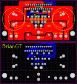
Here is an image of my revised layout, making it a bit deeper (0.05" deeper), and moving the output GND pad down more. I positioned the input terminals closer to the middle to keep the GND trace as thick as possible.
Any comments?
(ignore the dots in the the planes, as they are solid, but display differently in the screenshots. I also haven't added heat traces yet)
--
Brian
Any comments?
(ignore the dots in the the planes, as they are solid, but display differently in the screenshots. I also haven't added heat traces yet)
--
Brian
Attachments
Just a question won't PG+ and PG- create ground loops if you connect them both?
And like I mentioned previously, in parrallel mode, this chip would become unstable without a very closely located film capacitor, I don't know if it would do it with this layout, but it would be simple to add the pads just in case.
Sébastien
And like I mentioned previously, in parrallel mode, this chip would become unstable without a very closely located film capacitor, I don't know if it would do it with this layout, but it would be simple to add the pads just in case.
Sébastien
tool49 said:Just a question won't PG+ and PG- create ground loops if you connect them both?
Sébastien
The 2 PG inputs are from the power supply board, which uses dual bridge rectifiers (8xMUR860), so there the ground reference for the bridges are obtained on the actual amplifier pcb, not creating a ground loop. The CGND goes to the central ground.
Here are pictures of an identical setup with the LM3875:
http://www.briangt.com/gallery/nigc-kit
--
Brian
Ahh I hadn't followed the previous order but it seems to be a good idea to keep it compatible with your previous power supply board.
Sébastien
Sébastien
tool49 said:
And like I mentioned previously, in parrallel mode, this chip would become unstable without a very closely located film capacitor, I don't know if it would do it with this layout, but it would be simple to add the pads just in case.
I've built it without caps and it's more stable than LM3875.
To me the board is too wide (on a smaller side).
Great then it was my layout! I think I'm just gonna scrap my ten pieces of board. When is the group buy going to launch? I can hardly wait 🙂
Sébastien
Sébastien
Leaving a place for a couple film caps as a bypass wouldn't be a bad idea. You can always point-to-point wire them in but if you leave a couple extra pads across the 1000uF caps people can experiment with different bypassing options. The National Tech notes have a 1000uF electrolytic bypassed by a 10uF MKP & then a 0.1uF ceramic. I'm not so sure I'd use the ceramic but maybe a silver mica which is good at high frequency would be something worth giving a try.
Peter.... have you experimented with bypassing the electolytics on the LM3875s?
Peter.... have you experimented with bypassing the electolytics on the LM3875s?
I never liked bypassing. The only bypass that worked were 4.7u BG N caps on rectifier board. It wasn't that much for stability issues as for better sonics.
If no space for small caps on this board, one can alway attach any caps in parallel with big electrolytics underside. I believe that placing them in a usual space on board, will compromise optimum layout.
If no space for small caps on this board, one can alway attach any caps in parallel with big electrolytics underside. I believe that placing them in a usual space on board, will compromise optimum layout.
- Status
- Not open for further replies.
- Home
- Amplifiers
- Chip Amps
- LM4780 pcb layout and others