Re: Groundwork...
On your board, there is one commom groundplane and signal ground is shared with output ground. Redaing the post below this may not be the best approach. Separate those grounds and use separate track to connect them.
It seems to me that positioning PS caps at both, extreme ends is most convenient setup. On my board the distance between grounded leds of caps is less than 2", which shouldn't be that bad. The space between caps allows to place the rest of the components, allows access to mount the chip, and overall creates pretty compact layout, with minimum signal routing.
The input and signal grounds are run separately, and connected to this power ground at one point only (with separate track).
This type of layout was done with other board and the was no sign of performance suffering.
The only other way, I could see how this could be improved is bringing the caps together and mounting components underneath, but this introduces some limitation in implementation.
For instance with currently suggested layout, the PS caps can be mounted on both sides and the chip can be mounted on both sides (pins has to be formed for that, but it's not a problem). My Patek amp uses a board where chip is mounted on opposite side. If resistors were there, it wouldn't be possible.
digi01 said:thank you peter,It seems that the smaller and adaptation are directions in the future. . .
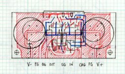
this is final layout,I use balance mode with + - input terminal,it
On your board, there is one commom groundplane and signal ground is shared with output ground. Redaing the post below this may not be the best approach. Separate those grounds and use separate track to connect them.
ALW said:Some advice for you guys - shorten the electrical path between the PSU reservoir caps 0V point.
Some of the boards above have them at extreme ends of the PCB, with a ground plane connection running across the board. You then have sensitive low-level signals referenced to a point with high current flows and finite impedance.
There will be significant current flows across the ground plane as a result of this, and depending upon how the rest of the connections go to ground this will likely introduce audible, and measurable, effects.
Ground rarely is ground, in reality. All traces and planes have finite impedance, it's worth considering this more closely.
Andy.
It seems to me that positioning PS caps at both, extreme ends is most convenient setup. On my board the distance between grounded leds of caps is less than 2", which shouldn't be that bad. The space between caps allows to place the rest of the components, allows access to mount the chip, and overall creates pretty compact layout, with minimum signal routing.
The input and signal grounds are run separately, and connected to this power ground at one point only (with separate track).
This type of layout was done with other board and the was no sign of performance suffering.
The only other way, I could see how this could be improved is bringing the caps together and mounting components underneath, but this introduces some limitation in implementation.
For instance with currently suggested layout, the PS caps can be mounted on both sides and the chip can be mounted on both sides (pins has to be formed for that, but it's not a problem). My Patek amp uses a board where chip is mounted on opposite side. If resistors were there, it wouldn't be possible.
Re: Re: Groundwork...
No it doesn't have to be. At least, that what National's evaluation board suggests😉
mAJORD said:
Is this in relation to star grounding? are you saying the star point should be as close to the cap as possible?
No it doesn't have to be. At least, that what National's evaluation board suggests😉
Star point, sort of
Take a look at 'Digi01's' PCB above.
The PSU caps are at each end of the PCB. The 0V return for each cap goes to a ground plane.
Between two caps we have a current path, from each cap to the incoming ground connection to the PCB. Also between these points there are a large number of ground connections - every single one of these will be at a slightly different potential at any given point in time.
If you start to reference signals to these points you run the risk of adding errors to them, related to the current flow through the ground plane at any given point in time.
As a useful tool it can be useful to analyse extremes, imagine each 0V return, from every component on the PCB, had several 10's of ohms of impedance, then analyse the effects of this and whether it matters, in terms of error signals added to the amplifier input or output.
In my opinion a star point would be a better approach, but I'd still reduce the electrical length of the 0V return from each cap to the star point.
Andy.
I agree that digi's board is not optimised for ground routing. I already mentioned that above. National's board is using star ground, but the common connection doesn't seem to be very close to power ground.
Of course this was not an inspiration point for me😉
Of course this was not an inspiration point for me😉
It seems to me that positioning PS caps at both, extreme ends is most convenient setup.
Peter,
With minor exceptions, adding length to signal path connections will not degrade the performance to the level that the poor grounding arrangements can.
Andy.
ALW said:
Peter,
With minor exceptions, adding length to signal path connections will not degrade the performance to the level that the poor grounding arrangements can.
Andy.
You put caps any closer together, and you won't be able to unmount the chip without having to remove caps first. I really wouldn't like to go into mounting components on the bottom side, otherwise I don't see a way to keep the current size and reduce ground length. And to keep the board size small is very appealing. We still don't know for sure if reducing ground length will bring any subjective benefits. Can you be sure of that (without testing this particualr circuit first)?
Can you be sure of that?
That totally depends on whether it introduces errors to the signal you are amplifying, which isn't too difficult to determine by analysis.
My experience with PSU's tells me this sort of stuff is important, sonically. The reservoir caps and the speaker return represent the largest current flows into the ground line, you do not want these modulating input signals to the amp.
Andy.
ALW said:
The reservoir caps and the speaker return represent the largest current flows into the ground line, you do not want these modulating input signals to the amp.
I was under the impression that my current layout takes care of that.
I totally agreee with ALW that it's extremely important with ground, high current paths when you have it all on pcb. The resistance isn't zero.
Example: 100 micorohms and 10 A, how much voltage drop do you get by that? Compare this with the output voltage. This error voltage creates distortion products.
Example: 100 micorohms and 10 A, how much voltage drop do you get by that? Compare this with the output voltage. This error voltage creates distortion products.
peranders said:I totally agreee with ALW that it's extremely important with ground, high current paths when you have it all on pcb. The resistance isn't zero.
Example: 100 micorohms and 10 A, how much voltage drop do you get by that? Compare this with the output voltage. This error voltage creates distortion products.
You are forgetting that this is GC and the board will never see 10A currents.
Yes, that is good altough I would have tried to make the separation even clearer.Peter Daniel said:
I was under the impression that my current layout takes care of that.
When I see the original from National I think their pcb layout isn't 100% optimal, check the ground arrangement.
Peter
I wasn't critiquing your layout, which I've not looked at.
Are you sure?
The LM3875 limits at 5A but allows transients higher than this, which is hardly insignificant, the 3886 higher than this. I strongly suggest that there is every potential for you to see currents of this order, particularly with the 4780!
Then there's the currents that come from the reservoirs themselves, which are primarily limited by the Z of the caps. Again it's easy to see peak currents of this order, in a rectified PSU, with the amp at idle.
Andy.
I was under the impression that my current layout takes care of that.
I wasn't critiquing your layout, which I've not looked at.
You are forgetting that this is GC and the board will never see 10A currents.
Are you sure?
The LM3875 limits at 5A but allows transients higher than this, which is hardly insignificant, the 3886 higher than this. I strongly suggest that there is every potential for you to see currents of this order, particularly with the 4780!
Then there's the currents that come from the reservoirs themselves, which are primarily limited by the Z of the caps. Again it's easy to see peak currents of this order, in a rectified PSU, with the amp at idle.
Andy.
Re: Peter
In that case, "will hardly see" is probably more suitable.
I'm well aware that proper grounding is very important and in some cases may influence the performance by 30%.
But we shouldn't be forgetting that this is GC and simplified approach alone, gives a designer much better starting point than it is in case of more conventional amps, with big, multiple capacitors and discreet output stages. You can give much deeper analysis to the length and routing of ground planes in those cases as it will always be harder to do it properly (there).
In case of GC we are dealing with a simple ground plane, connecting two caps, where length of this plane is smaller than in most cases diameter of conventional filter caps used in regular SS amps. With tight layout, signal grounding is simple as well and connecting both shouldn't be comparable to a rocket science.😉
Regardless of that, I took with great consideration all mentioned points and will use them in my more complicated designs😉
ALW said:
Are you sure?
In that case, "will hardly see" is probably more suitable.
I'm well aware that proper grounding is very important and in some cases may influence the performance by 30%.
But we shouldn't be forgetting that this is GC and simplified approach alone, gives a designer much better starting point than it is in case of more conventional amps, with big, multiple capacitors and discreet output stages. You can give much deeper analysis to the length and routing of ground planes in those cases as it will always be harder to do it properly (there).
In case of GC we are dealing with a simple ground plane, connecting two caps, where length of this plane is smaller than in most cases diameter of conventional filter caps used in regular SS amps. With tight layout, signal grounding is simple as well and connecting both shouldn't be comparable to a rocket science.😉
Regardless of that, I took with great consideration all mentioned points and will use them in my more complicated designs😉
Peter.... great work. We have the Wiki started for the National Eval board but there seems to be a lot of interest in optimizing it similar to Brian's 3875 efforts. Why don't we flesh out a final design here and vote on it for the Wiki order. Once we finalize on the design I can set up a PayPal order form and/or a credit card ordering page.
I'd consider the following most important.
#1. Flexible layout so that it can be built bridged, parallel & stereo.
#2. Best possible grounding scheme.
#3. Small form factor.
Assumptions:
#1. NFB resistor soldered direct to chip.
#2. All optional components left off but with solder pads to wire them point-to-point if needed or desired.
#3. Cut off NC pins to give more layout flexibility and maximize trace sizes.
I've been playing with EAGLE Light (a decided newbie at this) and I've stripped off the output resistors and shunt resistors because they are easy enough to wire point to point. The shunt can be wired on the input RCAs and the output resistors direct to the binding post. This helps me with layout because I'm a beginner and it offers more flexibility in keeping the grounding scheme optimal.
Any thoughts or comments on the above are welcome. If you disagree on my list of assumptions or priorities let's hear from you.
Hi, this may seem like a bit of a stupid thing to say, but aren't PCB's for mounting components?
It seems to me that if you are going to start wireing half the components in the circuit point to point then you may as well go the whole hog and do the rest that way to. IF it were up to me, I would try and keep all of the components needed on the board (including the NFB resistor, as it won't mount nicely like it does on the LM3875).
I think in this respect Peter's board fits quite well, as it is a now a proven configuration with a design similar to the existant one (which has been proven to work well for almost everyone) and will alow similar of different input signals for each chip with the addition of a simple jumper lead.
Kevin Haskins said:
#1. NFB resistor soldered direct to chip.
.... and I've stripped off the output resistors and shunt resistors because they are easy enough to wire point to point. The shunt can be wired on the input RCAs and the output resistors direct to the binding post.
In this case you are left with a board containing just the chip and 2 filter caps 😉
The board that I'm proposing here is optimised for parallel configuaration only. Few reasons for that: first of all, using the board for stereo operation doesn't make sense, as two separate LM3875 will sound better and provide better separation.
If the current board was optimised for bridged operation, unnecessary connections and jumpers would have to be introduced and this degrades layout again. For somebody who wants to use bridged amps, they should also seriously consider parallel setup and use simply 2 boards for that, (or just one amp on ea board).
I will be pursuing this design both commercially and on the forum as a part of group buy (if enough interest is presented). I guess the best person to take care of that is Brian, as he already has experience and success with other kit. I might help him with distribution though😉
But I don't see a reason why another board shouldn't be designed, which is suitable for all 3 configuration (stereo, parallel, bridged) and accomodates additional parts from National's layout.
Go for the professional approach, everything on the pcb, only "air" mounting when all other options are out.bigparsnip said:Hi, this may seem like a bit of a stupid thing to say, but aren't PCB's for mounting components?
bigparsnip said:Hi, this may seem like a bit of a stupid thing to say, but aren't PCB's for mounting components?
It seems to me that if you are going to start wireing half the components in the circuit point to point then you may as well go the whole hog and do the rest that way to. IF it were up to me, I would try and keep all of the components needed on the board (including the NFB resistor, as it won't mount nicely like it does on the LM3875).
I think in this respect Peter's board fits quite well, as it is a now a proven configuration with a design similar to the existant one (which has been proven to work well for almost everyone) and will alow similar of different input signals for each chip with the addition of a simple jumper lead.
For my use the main advantage of the PCB with this chip is that you can easily supply solder pads for input, output & power and mount the chip in a secure way. Also you can create a good star grounding point. It also simplifies some of the assembly. For many parts though it is just as easy to solder them elsewhere and it doesn't effect performance to solder a shunt resistor from the RCA hot to ground nor the output resistors to the binding post. It doesn't end up looking like a rat's nest of components and the critical grounding is taken care of by the PCB layout. I don't have any reason for putting them external to the board though other than simplicity in designing the PCB & flexiblity in how it is used.
Having said that though I'm aware I'm at the far end of the spectrum in terms of what to put on the board. 🙂 If it were done with more components rather than less I wouldn't loose any sleep over it. The flexiblity issue could be resolved by simply coming up with different PCBs for bridged, parallel & stereo mode.
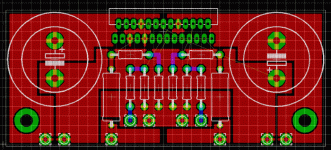
Ok, I have done a quick layout check in eagle, and I have come up with the component layout below, which fits all of the necessary parts onto the board (I haven't put in the mutting circuits, or wired it up yet but that shouldn't be a problem) for a stereo or paralal amp.
Obviously, none of the parts I have on the board are quite the right size yet, as it will mean creating new library files for most of them (and I don't have time to do that tonight, but probably tomorrow afternoon, if people are still intrested), and I'm not sure what the selection of components will be for this.
But anyway, the whole thing as it is at the moment measures 3.4 by 1.4 inches (compared to 2.9 by 1.2 for brians original boards) and should be able to shrink a little once I have the corect sizes for all of the componets in there (I esspecialy think the main PSU cap markings may be a bit large). Also, there are a few more padds to add for various conections, as well as a jumper or two to enable paralel opperation of the board, which should be there in the next day or so too.
So, people what do you think? is this about right for most of you, or will it need changing a lot to meet peoples needs?
(oh, and I have no intention of making these myself at the moment, as I'm just about recovering from the rectifier PCB thing, but if someone else wants the gerber files or something to get the boards produced then I guess that would be fine with me).
Attachments
- Status
- Not open for further replies.
- Home
- Amplifiers
- Chip Amps
- LM4780 pcb layout and others