...
He goes on to show arrangements that manage to satisfy 3 and then 4 of the objectives using a 4 layer PCB.
8 layers seem to be required to satisfy 5 of the 6 objectives,
and 12 or 14 layers to satisfy all 6.
...
😱
😕
Better every time.
If it was mine, I would probably be forced to make the PCB bigger, to have more on board capacitance per amplifier.
Would I get better channel separation, if I put series diodes to each rail to each amplifier from the power input connections?
Would I get more or less problems if I tried to share the same reference point for each channel, i.e. both channels shared the same Audio GND?
Member
Joined 2009
Paid Member
It shouldn't be so complicated, law of diminishing returns for all the time spent - wondering if this is a case of design by committee - isn't there a Russian joke about why some camels have two humps...
Me I'd use:
Layer 1 (top) for signals, minimise use of vias with SMD components, getting the majority of signals on this layer (this is were good placement comes in).
Layer 2 GND, all grounds, slot to avoid power interfering with signal/low current ground
Layer 3 power
Layer 4 Any signals that cant be done on layer 1/GND copper pour
If you are using a PCB manufacturer you can use vias down to 0.6/0.3mm easily depending on the spacing requirements.
As well as Henry Ott, there is information from Texas and Linear for analogue layout and from the likes of Howard Johnson for high speed....
Last edited:
I think that the latest PCB version should now achieve datasheet performance. So I'll stick with 2 layer version for now. Tomorrow I'll post regulated power supply with use of LT108x linear regulatos family.
Best Regards,
Aleš
Best Regards,
Aleš
I think that the latest PCB version should now achieve datasheet performance.
Assuming you have a pair of ceramic decoupling caps on the bottom of the board, yes. You need some decoupling at frequencies above 10-100 kHz where the electrolytics aren't effective.
Why not use SMD for the feedback resistor? You should be able to find a 1206 size component that can handle the power... Same question could be asked for the input cap. I'm sure you can find a nice Nichicon Muse audio cap in surf mount.
Also, I suggest widening up the output trace. You're paying for the copper anyway. Might as well use it.
My comments refer to what I believe is the latest rev. in Post #79.
~Tom
Me I'd use:
Layer 1 (top) for signals, minimise use of vias with SMD components, getting the majority of signals on this layer (this is were good placement comes in).
Layer 2 GND, all grounds, slot to avoid power interfering with signal/low current ground
Layer 3 power
Layer 4 Any signals that cant be done on layer 1/GND copper pour
....
You are an increadible reasource!
Please comment of these layers, oh Master Stacker! (like a high-speed-signal-Sensei!)


from:
View attachment zd-50-rev-d712107-main-board.pdf

Whilst I am a big fan of ground planes there are some issues with using them on power amplifiers.
The input and output ground currents need to be isolated as far as possible or you can end up with a positive feedback loop causing oscillation.
In your current design the op ground current will return across the ground plane to the bulk decoupling capacitors as a half wave rectified version of the audio signal. In this design it will flow back through the sensitive input and feedback ground region.
You have connected the input and output grounds together
From TI Datasheet
"When designing a layout, it is important to return the load ground, the output compensation ground, and the low
level (feedback and input) grounds to the circuit board common ground point through separate paths. Otherwise,
large currents flowing along a ground conductor will generate voltages on the conductor which can effectively act
as signals at the input, resulting in high frequency oscillation or excessive distortion. It is advisable to keep the
output compensation components and the 0.1 μF supply decoupling capacitors as close as possible to the
LM3886 to reduce the effects of PCB trace resistance and inductance. For the same reason, the ground return
paths should be as short as possible."
Also (but not mentioned in the TI datasheet) placing ground plane under a power amplifier can cause problems with the parasitic capacitance from the PCB coupling the +ve or -ve input and the high current and voltage output together at very high frequencies causing HF instability. Since the LM3886 can have loop gain to 8MHz this is a possibility if at any frequency upto 8MHz there is enough capacitance to couple signal to the +ve input or enough phase change to invert the signal and couple it into the -ve input you will get instability. In most circumstances this will be fairly low level and without a high speed scope you might never know it is there but it will heat the chip up and cause some sound degradation.
I would recommend not using plane under the chip. I would also recommend thinking about how the current will return from the output ground to the bulk decoupling capacitors and then onto the ground wire.
You may need to rearrange your decoupling capacitors and split the planes to separate the return paths to the ground wire for the large signal power returns and the input and feedback signal ground currents.
Having designed or been design manager for several audio power amplifier at several HiFi companies (Meridian / TagMclaren / ARCAM) I don't normally use ground planes on power amplifiers. Although we did use them on some of the ARCAM amplifiers for the input stage and another one on multi-layer boards. They were split to isolate the high currents from the low currents and careful consideration was take of the path from the decoupling capacitors and ground point to consider how the rectified halves of the audio signal flowing from the positive and negative rails would return to avoid it coupling into the low level input signals or the feedback point. Using planes with relatively low frequencies but high currents and voltages in the same circuit as low level signals is difficult and whilst it can have advantages, the two designs using planes were done by better power engineers than me and both required more than one iteration to optimize the performance.
I would always recommend planes for pre-amplifiers, RF and mixed signal / digital circuits. (although you still need to consider the return paths)
The LM3886 is quite forgiving so you have a good chance of getting away with it but I doubt it will be the optimal design.
If I was design it I would be splitting the ground returns into the input and output grounds and returning them to the center point on the decoupling caps in a somewhat simplified version of your initial layout. You don't need a separate return for every signal and a few wider but well selected combinations is better than every return coming back separately. You should also consider that the the noisy region for the high currents is between the current flowing from the supply and its return ground so ideally you want the track too the decoupling cap and the track going back again to be next to each other or on top of each other (This is sometimes impossible to arrange and compromises have to be made) it is OK to share the ground with the positive and negative rail capacitors but you don't want these passing parallel to the input signals for any significant length as the cross coupling can cause instability or pick up of the rectified half of the audio signal can cause distortion. (this is all more significant in discrete component designs but the same principals apply for chip amplifiers)
Regards,
Andrew
The input and output ground currents need to be isolated as far as possible or you can end up with a positive feedback loop causing oscillation.
Actually, connecting the input ground to the output ground provides the best performance. I have shared the data to back up this claim in the LM3886 P2P vs PCB thread.
"When designing a layout, it is important to return the load ground, the output compensation ground, and the low
level (feedback and input) grounds to the circuit board common ground point through separate paths.
That doesn't exclude a ground plane, though. If laid out properly, you can create a star ground using a plane. Granted, you won't get the giant spider ground, but by careful placement of the components on the board you have full control of where the current will flow. Nothing prevents you from having one section of the board be a quiet ground, connecting with a low-impedance trace to the ground at the output connector. The advantage of the plane over the spider ground is that the plane offers much, much lower inductance, resulting in much better performance at frequencies above 1 kHz.
~Tom
Having either separate planes or strategic splits in planes is common practice on many high power analogue control boards (basically amplifier boards, be they audio or some other form of control), one area where this is becoming very prevalent is in automotive control, where you can have sensitive analogue section, digital and high power amp outputs for various controls. This is where good PLACEMENT practice (the most important skill) in PCB design comes into play. During placement even if you are going to join the GNDs it helps to have separate AGND, DGND and POWER-GND and have them displayed as different colours. Then during placement you can use these colours to help group the components in relation to their GND signals. Then you can fine tune placement within these main groupings.
These sort of designs are very common, motor controls, audio etc. all follow the same basic topology, small control signal in large control signal out and separating the high power from the low power is critical... That said I would minimise the amount of separation to high and low level ground, analogue and digital I prefer to separate my careful placement, but them I tend to work on slightly more complex designs where trying to determine where to join AGND and DGND is hard to do as there are often several devices.
On single chip designs such as these though the rules can be twisted more, these devices (with the correct decoupling) can be quite forgiving, they are also used quite extensively for other control functions outside audio.
Another technique that I have mentioned is using Balanced Routing for the input signals, again this can be a very useful technique for low level analogue and for separating the input signal and its return from the rest of the boards GND, joining the two together (if required) at the devices input pin.
Currently doing some fun analogue digital designs, the control boards for the flight refuelling systems, where all the above techniques are being used.
A last though, for power outputs on a PCB you do the same as you would with wires, either two very large tracks or copper pours (often required for the power requirements and to avoid excessive heating) that mirror each other, kept as short and compact as possible, with the minimum distance from the active driving device to the output connector and as far away from any sensitive circuitry as possible. Again minimise how many grounds you have, this simplification does make life easier power ground and signal grounds are all you need for the majority of designs, especially on simple audio designs (simple in terms of component count and number of channels, usually 2)🙂
Last edited:
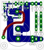
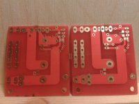
I've added separate pictures for top and bottom layer. I'll stick with tantalum capacitor on the input, as said before, to me it has most neutral sound.
For power supply I'll be using two identical PCBs connected together creating +/gnd/- lines.
BR,
Aleš
For power supply I'll be using two identical PCBs connected together creating +/gnd/- lines.
BR,
Aleš
Attachments
Last edited:
You are an increadible reasource!
Please comment of these layers, oh Master Stacker! (like a high-speed-signal-Sensei!)
View attachment 460468
View attachment 460469
View attachment 460470
View attachment 460471
from:
View attachment 460467
Nice layout. I am impressed, we do similar layouts and some so called pro designers we use would not do as good.
Being pedantic though there are some areas of the placement that can be tweaked to get the interconnections between components minimised. But they are minor and you have most of the routing on separate layers with the minimum of signals passing through vias. Unlike many designs we see I suspect some real thought has gone into placement, which has paid of in terms of routing and the neatness in the routing. An example of fine tuning would be turning R67 round so the connection between it C59 is direct (the other connection has to already meander so a little more wont make any difference. D8 I would also place equidistant and as near to the pins of the relay, think of it as a sort of decoupling device for back EMF. These points are rather pedantic but are the sort of things I worry about on my layouts, it is this fine tuning that just adds that sparkle to your layouts and differentiates them from mundane.

Tom sorry for my confusing description. I didn't say the input ground and output ground should not be connected together. I said they should be isolated as far as possible. This was a direct response to the PCB layout in which they are not connected together at the ground entry point (as in your design) they are connected together a significant distance from the psu ground entry so will share ground impedance. In this design because its a plane it probably won't make much difference but it would be better to have separate return paths for the input ground and the output ground to the PSU ground.
I also did not say you could not use a plane, I was responding to this design which does not full fill those suggestions.
Andy
I also did not say you could not use a plane, I was responding to this design which does not full fill those suggestions.
Andy
Nice layout. I am impressed, we do similar layouts and some so called pro designers we use would not do as good.
Being pedantic though there are some areas of the placement that can be tweaked to get the interconnections between components minimised. But they are minor and you have most of the routing on separate layers with the minimum of signals passing through vias. Unlike many designs we see I suspect some real thought has gone into placement, which has paid of in terms of routing and the neatness in the routing. An example of fine tuning would be turning R67 round so the connection between it C59 is direct (the other connection has to already meander so a little more wont make any difference. D8 I would also place equidistant and as near to the pins of the relay, think of it as a sort of decoupling device for back EMF. These points are rather pedantic but are the sort of things I worry about on my layouts, it is this fine tuning that just adds that sparkle to your layouts and differentiates them from mundane.
Tell me more, kind sir. This is NOT my layout; I am merely a gatherer of good information ...
Tom sorry for my confusing description. I didn't say the input ground and output ground should not be connected together. I said they should be isolated as far as possible. This was a direct response to the PCB layout in which they are not connected together at the ground entry point (as in your design) they are connected together a significant distance from the psu ground entry so will share ground impedance. In this design because its a plane it probably won't make much difference but it would be better to have separate return paths for the input ground and the output ground to the PSU ground.
I also did not say you could not use a plane, I was responding to this design which does not full fill those suggestions.
Andy
Well. I apologize if I misunderstood.
~Tom
not sure why you want to use a regulated supply.
If thats a lm317, it cant even supply current to a single channel of lm3886.
Do you want to use lm317 and 337 to create the dual rails on two of the same psu pcb. I dont think you can use the same pcb as their pinout is different.
If thats a lm317, it cant even supply current to a single channel of lm3886.
Do you want to use lm317 and 337 to create the dual rails on two of the same psu pcb. I dont think you can use the same pcb as their pinout is different.
i think you plan to use 138/338, so i guess you can ignore the above comment.🙂not sure why you want to use a regulated supply.
If thats a lm317, it cant even supply current to a single channel of lm3886.
Do you want to use lm317 and 337 to create the dual rails on two of the same psu pcb. I dont think you can use the same pcb as their pinout is different.
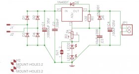
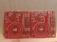
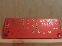
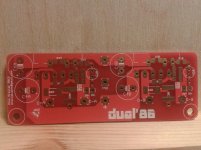
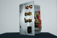
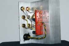
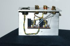
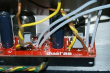
Amplifier is built and running. Dynamics are really good compared to the solid state amps. I heard how much effect had small heatsink on the sound, especially dynamics. Current heatsink has temperature of 8°C more than the ambient temperature (approx. 20°C). Though I am still thinking that I would add copper bar between chips and aluminum heatsink.
As seen on the pictures I used MKP1837 100nF for zobel filter (had them in stock and I thought they would be better than the WIMA smd caps) and 470uF filtering capacitors instead of 100uF.
BR,
Aleš
p.s. Current power supply is built from two Meanwell DR-75 PSU working at 24V.
As seen on the pictures I used MKP1837 100nF for zobel filter (had them in stock and I thought they would be better than the WIMA smd caps) and 470uF filtering capacitors instead of 100uF.
BR,
Aleš
p.s. Current power supply is built from two Meanwell DR-75 PSU working at 24V.
Attachments

- Status
- Not open for further replies.
- Home
- Amplifiers
- Chip Amps
- LM3886 with SMD components