When is amplifier is in circuit (always is kind of amplifier) you have input signal, feedback and ouput signal. Those three signal must have the same referent point, ground. Whats mean same, you must no have any current between those points, or you must put signal (high impedance) ground behind power output ground. Charging capacitors causes voltage drop on ground trace, no matter how small, if is signal ground and output-feedback ground on different side, you have amplification voltage what capacitors causes.
What is mean when you have opamp, small power load? You always have capacitors and charging currents, and you always have any voltage drop at ground trace. If you take signal and output ground from wrong points you have 100Hz buzz in sound.
I`ll try draw one situation and post here.
What is mean when you have opamp, small power load? You always have capacitors and charging currents, and you always have any voltage drop at ground trace. If you take signal and output ground from wrong points you have 100Hz buzz in sound.
I`ll try draw one situation and post here.
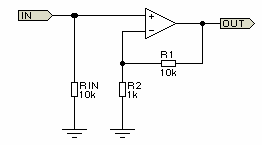
Here is simple example. Rin is connected at ground. The voltage of the input signal relative to the point on ground of Rin is our useful signal. This point is reference point for non inverting input. Ground of R2 is reference point of inverting input. If You have any, no matter how small, voltage between those points, after amplifier you have increased this voltage and this is noise. If is at that trace between R2 and Rin track for charging currents, problem is much much bigger. power supply is housed on the other side tiles but hum is audible. I cut the ground plane and make a line for charging capacitor, line to the voltage stabilizer and hum is missing. You can use ground plane only when is ground plane is connected at signal ground only at one point. so great gnd although pick interference is space they will all be at ground potential and it is us a reference point and we do not care what's going on around. You must have had a situation that you amplifier hums when not connected signal. This is because your metal enclosure of amplifiers receive interference from space and transmitted as an antenna on the unprotected signal cables. By connecting enclosures for gnd even with a resistor will eliminate hum with no connected inputs. The same thing with ground plane when is connected at signal or output ground.
Attachments
Last edited:
That makes sense, well assuming you mean R2 not R1, so you are saying that ground must be lowest possible impedance between those points? Everyone agrees with that.
Yes R2. i corrected the post That ground can be at kohm if you have not current between those points. Must only be careful when positioning components that physically between these points there is no current.
Last edited:

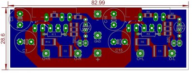
...and this is how current PCB looks like. I was thinking, maybe I could extend PCB a few mm behind LM3886 so the Vss line could be moved further away from the left input circuitry. In order for Lm's to reach heatsink, copper or aluminum bar could be used to fill in the gap.
Attachments
Would the OP post a schematic?
Someone brought up that there needs to be a DC path from each input on the LM3886. That's a good catch! Personally, I also prefer to tie the input end of the capacitor to ground via a resistor. With a schematic this would be easy to draw...
That is certainly true. That's one of the tradeoffs you make when putting two amps on one board. You could estimate the impedance between the left channel and the supply caps to quantify the error voltage that develops because of this kind of layout. I strongly suspect, however, that the ripple voltage that develops in the power supply due to the current draw of the left channel will introduce a much larger error voltage than that developed across the VCC/VEE pours. As long as this amp is built as a stereo amp, that will be the case.
Not really... It just moves the issue closer to the supply.
That's the drawback of using an amp with low PSRR... (hint 🙂)
It's difficult to get a good layout. Period... The layout in Post #54 is actually close to optimal for the left channel. The right channel is slightly sub-optimal due to the location of the supply connector. However, I think we're counting Gnat Farts here.
~Tom
Someone brought up that there needs to be a DC path from each input on the LM3886. That's a good catch! Personally, I also prefer to tie the input end of the capacitor to ground via a resistor. With a schematic this would be easy to draw...
Just noticed the separated +ve and -ve feeds around the left amp that will see interference from rail pulses due to current demands of the right amplifier.
That is certainly true. That's one of the tradeoffs you make when putting two amps on one board. You could estimate the impedance between the left channel and the supply caps to quantify the error voltage that develops because of this kind of layout. I strongly suspect, however, that the ripple voltage that develops in the power supply due to the current draw of the left channel will introduce a much larger error voltage than that developed across the VCC/VEE pours. As long as this amp is built as a stereo amp, that will be the case.
Two completely separate triplet feeds to left and right channels will solve much of this.
Not really... It just moves the issue closer to the supply.
That's the drawback of using an amp with low PSRR... (hint 🙂)
It is really difficult to get a good one chip layout, I gave up on two chips.
It's difficult to get a good layout. Period... The layout in Post #54 is actually close to optimal for the left channel. The right channel is slightly sub-optimal due to the location of the supply connector. However, I think we're counting Gnat Farts here.
~Tom
I understand the move from resistance path to inductance path as the frequency increases. What happens when there are multiple paths of each type?
There is no change or move from resistance to inductance. There is only impedance. The impedance is a frequency-dependent resistance.
Z(s) = R + s*L, where s is complex frequency (s = j(2*pi*f)). Note that electrical engineers use j for the imaginary part of the complex number, whereas mathematicians use i. Complex number - Wikipedia, the free encyclopedia
At low frequencies, the R term dominates as s*L << R. At high frequencies, the s*L term dominates as s*L >> R. Both terms are always present.
With multiple impedances in parallel, the current is divided according to the ratios between the impedances. This is similar to the way a purely resistive current divider works. As we now know, all paths have impedance, hence, are frequency dependent, the current divider will be frequency dependent. At this point the math starts becoming rather hairy. If you want to play with it, I suggest setting up a simulation with a few L+R paths in parallel. Drive them with an AC voltage and look at the current though each path vs frequency.
~Tom
Last edited:
Not exactly what I had meant at the time but if you look at the PCB on #66 you can expect the LF current to flow between O-R and the (power) GND while the higher frequencies it will flow between O-R and C1/C2.
Last edited:
I didn't suggest that you didn't. (reread my first word)
Current follows all available paths, but much of the current follows the paths of lowest impedance. At low frequencies most of this impedance is resistive. While at high speed most of the impedance is inductive.
Sorry 😀
You could allow yourself to be inspired...
http://www.diyaudio.com/forums/chip-amps/268027-mini-86-lm3886-smd.html
~Tom
http://www.diyaudio.com/forums/chip-amps/268027-mini-86-lm3886-smd.html
~Tom
So you're suggesting to stick with mono PCB?
Aleš
No. Make it stereo!
As you are planning to order these from a PCB manufacturer, why stick to only 2 layers?
Make it in 4 layers!
Here (on this forum) you have super skilled guys to help you in designin a SUPERB stereo PCB for the 3886. Better PCB than you kan get in any kitt anywhere.
No. Make it stereo!
As you are planning to order these from a PCB manufacturer, why stick to only 2 layers?
Make it in 4 layers!
Here (on this forum) you have super skilled guys to help you in designin a SUPERB stereo PCB for the 3886. Better PCB than you kan get in any kitt anywhere.
Yes I plan to order these from PCB fab. I suppose I can make it 4 layer.
Some thoughts about 4 layer PCB:
1. GND layer should be layer 2?
2. What would be better: to make supply lines on layers 3 and 4 or just on layer 4?
3. For decoupling caps would it be then better to use through hole capacitor or SMD with inner connection from layer 4 to layer 2?
But then would it really be worth it doing it and if the performance would drastically improve....
BR,
Aleš
Last edited:
signal ground on 1
low current signals on 2
ground on 3
power on 4
ground on 5
power on 6
etc .....
High current signals on which layer?
H.Ott gives six objectives to be aimed for on multi-layer PCBs.
Two pages later he show a 4 layer and an improved 4 layer arrangement and concludes with
"this configuration satisfies two of the six objectives."
He goes on to show arrangements that manage to satisfy 3 and then 4 of the objectives using a 4 layer PCB.
8 layers seem to be required to satisfy 5 of the 6 objectives,
and 12 or 14 layers to satisfy all 6.
He takes 35 pages (chapter 16) to explain PCB stack up and from that I know I cannot design multi-layer PCBs.
Last edited:
signal ground on 1
and from that I know I cannot design multi-layer PCBs.
Me neither... ;-)
Im just on average guy. I know nothing about multilayers...
There was an super-excellent state of the art money no object amplifier, i had the honor to closely follow its developement process. Unfortunately i just can not tell what.
I did not design the PCB. It was left to those who actually knew something about something.
It has 4 layers organized like this:
top layer: SHIELD! for everything inside.
bottom layer: SHIELD! for everything inside.
Top layer has the smd components and shortest possible leads between them. If longer tracks was needed, go inside, and put shields around them for protection.
Inside layers: POWER. On both 2 and 3. And speaker output.
Note. There is no power PLANES inside. They too are tracks (WIDE though, 1 inch minimum) but kept away from the sensitive circuitry (or should i say, the sensitive circuitry was kept away from these). Most of the copper is for GND. Grounds everywhere connects in one place, the "ideal zero". And you can already guess what that place might be.
And what it all then became? Three words: O-M-G!
How much does it cost then? Also three words: O-M-G!
Anyways,
my suggestion for this stereo 3886 is that start the process by putting the power input to the middle of the pcb. Then design two ABSOLUTELY IDENTICAL amplifier channels to both sides of that power connector. Every track must have the same impedance on both amplifiers, i.e. power tracks.
Shield the power tracks when going under the things that matters, or should i put it this way, shield the thing that matters, from the power tracks...
So you're suggesting to stick with mono PCB?
No. I'm suggesting that you implement the low-impedance grounding shown in the Mini-86 thread. In particular, notice the routing around the Zobel network and how Cz connects directly to the ground plane though a sizable via.
A good high-current, high-voltage op-amp (which is what an LM3886 is) is all about minimizing impedance, i.e. minimizing inductance and resistance.
There's no need for more than two layers in the PCB. I'm able to beat the data sheet performance of the LM3886 with a good 2-layer layout. I show the data in the LM3886 P2P vs PCB thread.
~Tom
Good read! Highly recommended!
Your awesome layout 😎 got me thinking about how the V+ is routed.

Is pin 1 the real V+ power pin compared to pin 5?
Are they shared?
Going to different parts of the circuit ?
?...?
The "Equivalent Schematic (excluding active protection circuitry)" doesn't show anything:

And only the first schematic even shows pin 5 ...
Does anyone have the full internal schematic of the LM3886? (My google-fu has failed!) 😉
Cheers and thanks,
Jeff
Is pin 1 the real V+ power pin compared to pin 5?
Are they shared?
Going to different parts of the circuit ?
?...?
The "Equivalent Schematic (excluding active protection circuitry)" doesn't show anything:
And only the first schematic even shows pin 5 ...
Does anyone have the full internal schematic of the LM3886? (My google-fu has failed!) 😉
Cheers and thanks,
Jeff
Last edited:
- Status
- Not open for further replies.
- Home
- Amplifiers
- Chip Amps
- LM3886 with SMD components