I guess I miss understood your statement. I understand the move from resistance path to inductance path as the frequency increases. What happens when there are multiple paths of each type?
We get horrible little loops and noise, depending on the system. Separate kit with heavy gauge mains leads and interconnects with a horrible braided screen is a prime example. The low frequency will use the earth connection as well as the braid and we have a ground loop. This is the problem, the dam stuff will seek out any path it can find, usually one that you haven't thought of or didn't know was there. The more complex the system and the more plugged into it the more likely you are to get bitten. That's what makes it all so much fun!!!
I have said the only place I see this spiders legs type layout is on DIY audio designs, no where else where analogue design is used.
Please tell what to use in place of spider legs? Split plane? Like one plane for signal, and then other for power?
Mark, three things that everyone needs to know about electricity:
1] Electrons are very lazy. They only move when forced to by voltage.
2] Electrons are very anti-social. They only get near other electrons when forced to by voltage.
3] Electrons know Ohms Law and all the other rules of electricity by heart. And they can instantly do all the math.
So in any situation they can determine what they need to do while avoiding other electrons and using as little energy as possible.
They will take all available paths, but their number will be inversely proportional to the impedance of each path.
Yes, I am very aware of how signals propagate and how electrons move (I have put up many posts illustrating this) as I do high speed PCB design and do signal integrity verification and simulation, I also use this software for power supply integrity:
http://www.algozen.com/DS_CADSTAR_LT_PowerIntegrityAdvanced_ENG_2011_10_05.pdf
So I probably understand more than many how signals travel round PCBs and on ground and power planes (do not forget that an adjacent power plane will act as the signal return path) as it is my job and I spend a lot of time on customers sites solving problems and doing critical layouts, such as analogue digital designs with over 4000 components. Currently doing the PCBs for the flight refuelling systems used in the world🙂
But as I said low frequency signals follow the path of least resistance as frequency increases the path changes to path of least inductance. I would hope you are not disputing this FACT?
Last edited:
Please tell what to use in place of spider legs? Split plane? Like one plane for signal, and then other for power?
Split planes are generally best, or routing the GND is acceptable, just don't go overboard as the previous posts illustrated with regard to the resistor and capacitor, they are related components so use the same gnd track for both instead of one for each device.
Split planes are generally best, or routing the GND is acceptable, just don't go overboard as the previous posts illustrated with regard to the resistor and capacitor, they are related components so use the same gnd track for both instead of one for each device.
Thank you. It makes a lot sense actualy. So one widest possible trace for all related components and ground pour for signal. Will try this in my Lm3886 pcb.
The main aim with the ground is to keep resistance and impedance as low as possible, resistance to minimise voltage drops due to current and inductance because it opposes current change, so a low impedance return path is what we are aiming for.
I didn't suggest that you didn't. (reread my first word)Yes, I am very aware of how signals propagate and how electrons move (I have put up many posts illustrating this)
Current follows all available paths, but much of the current follows the paths of lowest impedance. At low frequencies most of this impedance is resistive. While at high speed most of the impedance is inductive.But as I said low frequency signals follow the path of least resistance as frequency increases the path changes to path of least inductance. I would hope you are not disputing this FACT?

Suggestion: Make the ground plane solid and route the other connections on the top layer. Turn the VCC and VEE into pours and make them as wide as you can get them (lower the inductance).
~Tom
~Tom
I do not like ground plane because you can not be the judge which is the line of least resistance and where they are going currents.
That's the fundamental gap in understanding which prevents the average DIYer from using a ground plane. The average DIYer can easily trace a ground spider and visualize the electrons walking merrily single file down the trace singing Kumbaya. The average DIYer doesn't understand current density and has even more trouble visualizing the current density in a ground plane. Then you add misinformation and "so-and-so on the Internet once said..." and you have a real mess.
A good primer on grounding can be found in this paper: Successful PCB grounding with mixed signal chips.
In star-connection you determine the reference ground and amplifier is completely silent.
And if good performance at 50/60 Hz is your only goal, that's great. If you also want good performance above 1 kHz, you need to minimize the inductance, in particular of the reference ground used for the input connector. This, again, requires wide ground traces. The widest trace possible is a ground plane.
I've posted tons of data to support this in the LM3886 P2P vs PCB thread. You can also set up a simulation to explore the various ground connections. That'll will give you the same result.
~Tom
Last edited:
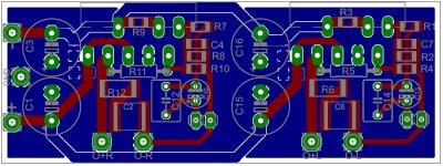
Getting better, but I still think it could be more compact. Plus I don't really like the fact that one chip is downstream of the other in power terms. The power to the second chip should connect to the other side of the first chip's caps, at the power inlet connector. Can't you contrive to keep V+ & V- closer together?
Sorry, cross post with tom, I don't intend to contradict his suggestions regarding pours, I'd prefer to see a single channel layout, duplicated.
Sorry, cross post with tom, I don't intend to contradict his suggestions regarding pours, I'd prefer to see a single channel layout, duplicated.
Last edited:
Just noticed the separated +ve and -ve feeds around the left amp that will see interference from rail pulses due to current demands of the right amplifier.
Two completely separate triplet feeds to left and right channels will solve much of this. Except the closeness of the right feed to the left input lines !
Two separate PCBs will probably perform better.
Pin5 has no effective HF decoupling.
C10 and C12 should be swapped.
Look at the Flow route through C12 and how far it is from the Return route.
Repeat for C14&13.
Last edited:
I dont think there is HF decoupling for the pin4 either?
I might try turning the input connector around just to see how the inputcircuirty would look then, or may be you have tried it and what you have now is the best alternative???
Anyways, the Zobel could connect to the ground plane directly (but this is still controversial on the forum, I think)... Returns to HF decoupling that is...
Edit:
And a couple of mounting holes wouldnt hurt either, would they? 🙂
Just for the sake of heavy cabeling...
Last edited:
That's the fundamental gap in understanding which prevents the average DIYer from using a ground plane.
~Tom
Ok. I with my average diy knowledge say that this board is not good and immediately to explain why. Charging the capacitor c15 and c16 with gnd input mass will cause due to pulse charge current the voltage drop at ground plane no matter how big and make a difference between gnd speakers and gnd of the input signal... I know when i must put resistor at ground behind amplification stage and when before the same stage. What mean that you have ground plane width like airplane runway, if you taking signal, or feedback from the wrong point.
After 20 years of designing industrial measuring devices believes this is at first sight quite clear. Whether and you.
Hi,
Any chance you can rephrase this slightly as really not sure what exactly you are trying to say. Sound like you are saying extra impedance is needed in some ground connections?
I think the input ground layout could be improved. In your layout there is a (Feedback) current that flows pin3/R11/R10/inputGND/O-R and R10/inputGND is also a part of the input circuit for the input return current.
C4/R8/R10 looks like a good reference point for the audio ground. One trace from R10 to input GND and one trace from R10 to O-R, you may need to move the input and C10+C12 to the right of the input trace.
It is really difficult to get a good one chip layout, I gave up on two chips.
C4/R8/R10 looks like a good reference point for the audio ground. One trace from R10 to input GND and one trace from R10 to O-R, you may need to move the input and C10+C12 to the right of the input trace.
It is really difficult to get a good one chip layout, I gave up on two chips.
Last edited:
Member
Joined 2009
Paid Member
- Status
- Not open for further replies.
- Home
- Amplifiers
- Chip Amps
- LM3886 with SMD components