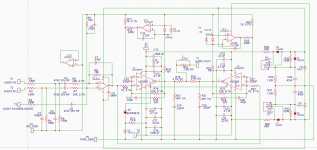
I would choose a Butterworth filter response as that's maximally flat. No need to introduce peaking in the DC servo. All the design equations are in Jim Karki's application note, which I linked to in Post #42. Note the equations can be simplified quite a bit if you impose a few constraints on the variables. See Appendix A (in particular section A.2.2). A Butterworth filter has a Q of 0.7 (1/sqrt(2) to be exact).I sketched some below. I don't know how to calculate those values. Used website here - https://www.embedded.com/analyzing-circuit-sensitivity-for-analog-circuit-design/
As for the gain: Do you absolutely need the amp to go to clipping at the reference level? Can the sources not provide more than -10 dBu and +4 dBu, respectively?
Tom

@gooduser: Note that -10dBV and +4dBu are supposed to be nominal levels, not maximum.
Since it's pretty uncommon for full-scale to be less than 1V RMS, I'd just set the gain to around 20V/V. A lot of consumer gear will actually do at least 2V RMS, and some pro gear is capable of more than 10V RMS (balanced).
Since it's pretty uncommon for full-scale to be less than 1V RMS, I'd just set the gain to around 20V/V. A lot of consumer gear will actually do at least 2V RMS, and some pro gear is capable of more than 10V RMS (balanced).
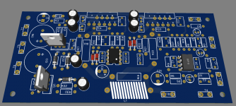
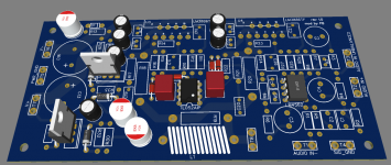

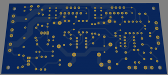
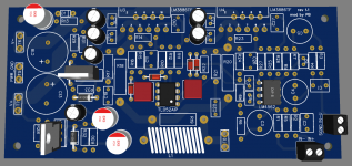
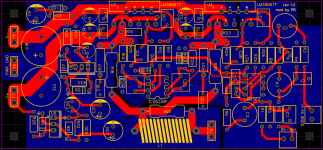
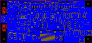
You'll have more fun assembling the board if you rotate the part designators so they're all facing the same way (or at least stick to two rotations - horizontal and vertical). Unless it compromises performance, I prefer to have all polarized parts oriented the same way. So all electrolytic caps have their anodes towards one edge of the board, for example. It makes assembly and debugging easier. I recommend using a square (or rectangular) pad on pin 1 of ICs. It makes finding pin 1 easier during debugging. The part often obscures the silk screen legend...
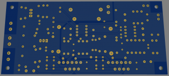
Spade connections are not commonly used for audio input. You're not likely to find a 1/4" spade that'll attach nicely to a microphone cable. How about a terminal block?
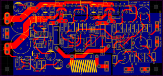
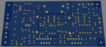
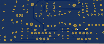
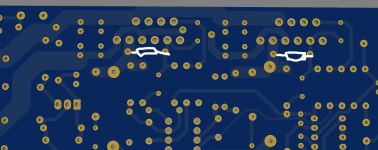
You may get a smidge better performance if you overlay V+ and V- along the top edge of the board on its way to U4. This maximizes the coupling capacitance between the two traces and minimizes the loop area between the traces. That should minimize the coupling into the feedback network around U3. The currents in V+ and V- for a Class AB amp are pretty nasty...
Tom
Spade connections are not commonly used for audio input. You're not likely to find a 1/4" spade that'll attach nicely to a microphone cable. How about a terminal block?
You may get a smidge better performance if you overlay V+ and V- along the top edge of the board on its way to U4. This maximizes the coupling capacitance between the two traces and minimizes the loop area between the traces. That should minimize the coupling into the feedback network around U3. The currents in V+ and V- for a Class AB amp are pretty nasty...
Tom
EasyEDA is super easy to use! It took me a few days to learn - I started with circuitbasics article on LM3886Well it looks great and you are light years ahead of me in using PCB software 🙂
Can I use TDK ceramics for C6 and C7 - those are 27pF?
I found some on Mouser - 810-FG18C0G2A270JNT6
I found some on Mouser - 810-FG18C0G2A270JNT6
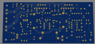
If you're looking for feedback on the layout it would be helpful if you'd post a screen shot like you did earlier. I need to see at least the top and bottom layers along with the silk screen.
Ceramic capacitors with C0G/NP0 dielectric would be good for values below 100 nF. X7R for those higher than 100 nF.
Tom
Ceramic capacitors with C0G/NP0 dielectric would be good for values below 100 nF. X7R for those higher than 100 nF.
Tom


I would say yes, each chip should be terminated correctly.Is it necessary to have 2 sets of Zobel networks?
You have to work on that electrical ground, in some areas it gets very narrow .
I plan on running just a wire between #7 pins of both chips
C10 and c27 are too large in size , c0g are very good and they take a fraction of that space.
Found TDK C0G 110pF capacitors on Mouser - 810-FG28C0G1H221JNT6
Will user those instead.
http://www.shine7.com/audio/bpa300.htmbpa300 amplifier . 2 Zobel , one for each half of the amplifier , same as
modulus686 , if Tom/Neurochrome.com can get involved in this .
modulus686 , if Tom/Neurochrome.com can get involved in this .
- Home
- Amplifiers
- Chip Amps
- LM3886 in parallel with servo circuit build attempt