Hi FF
First i have to excuse my self because I am actually too busy /unconsecrated to follow 100% the audio things. i am sorry. i will stop the science measurements and thank you for your polite feedback - that that is "useless for audio". sometimes i run with energy in the wrong direction.😀
.....................................................
Hi Chris,
Loosing our way in measurements is something that happens to us all. Today I investigated why the positive saturation level on my recent TDA7294 test-board was so poor. My boot-strap voltage looked strange and without the expected DC-bias level. I looked around but it remained weird. Then I realized that the oscilloscope probe used for the boot-voltage was AC-coupled, not DC-coupled as I assumed. Setting it to DC-coupling gave me a DC-bias but is was still strange as the levels did not match. I compared the output signal with the boot-strap voltage. Finally I realized that I had adjusted the variable gain on one channel for a photo the day before. This was why the scalings didn't match. With these corrections I realized that the boot-strap voltage was clamped before reaching the positive voltage rail, which is wrong. That caused the high-side power transistor to clip too early because the boot-strap didn't work. I need to change the chip.
This example illustrates that sometimes we have to sit back for a moment and think about what we actually measure and how we should interpret the results we get.
The more we are confused about the results we get, the more hectic we tend to become in our search for something that makes sense. We should then rather take a short break and re-start our tests in a more systematic way.
Keep up the good work, Chris!
When I find time, I will try to test in particular stability at low loop-gain for more of the chip-amps listed in the scheme in posting #510. The results I will post in a new thread https://www.diyaudio.com/forums/chi...fier-lm1875-tda2050-excluded.html#post6107694 in order not to pollute this LM1875/TDA2050 thread.
UTC-TDA2050V
The tests started with a loud “PAAFF”. A 4700uF/35V decoupling capacitor cap left its interior because the grooved top did not open. With only 18V. Such happens when you buy your capacitors too cheap.
Test of the TDA2050 was first done with a gain of -10 (inverting), within the recommended gain range. The results will describe performance for normal use. Further, the current limitation could be investigated.
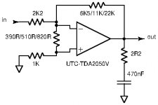
Image 1: Main components of the amplifier for the first tests.
To start with the current limiter, the TDA2050 is designed such that within the supply voltage range and with a 4 Ohm load, the current limit is only reached near voltage clipping of the sine-wave peaks. The load impedance had to be reduced to 3.2 Ohm and 2.7 Ohm in order to be sure it was current limitation I observed.
The limitation is, as Fred described it in posting #347, a combination of current level clamping and amplitude clipping reduction, probably controlled by the chip temperature. It actually functions quite well in combination but the two effects can be difficult to separate.
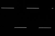
It is to be emphasized that the output signal is undisturbed until a bit beyond the peak current level of 5A, unless a high signal level is kept for long such that the chip temperature short after reduces the amplitude clipping level.
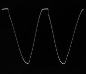
The current clamping level was reached some 7% above the 5A limit. With +/-23.5V supply voltage, current clamping was somewhat less controlled and with more instability than when the supply voltage was reduced a bit to +/-22V. +/-22V is a good supply voltage for the TDA2050.
Current clamping of the positive half-waves was almost perfect while clamping of the negative half-waves included a bit of instability, which is less important above the current limit. Soon reduction of the amplitude clipping level would follow. For real music, the current limit of 5A can be relied upon. For a constant sine-wave signal, a level of 4-4.5A should be assumed.
Image 2 shows how an undistorted sine-wave can be started with peak-levels above the 5A limit but just below the current clamping level.
Image 3 shows how the amplitude clipping kicks in some 2-3 seconds later and reduces the power to a sustainable level.
The UTC-TDA2050 can in real use deliver 25W in 8 Ohm and 40W in 4 Ohm, semi-continuously. That is better than the LM1875 and due to better handling of high currents by the TDA2050. An 8 Ohm load was trivial to handle so my results concentrated on 4 Ohm loading.
Results with a regulated +/-22V supply voltage, gain of -22 and a 4 Ohm load.
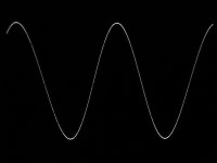
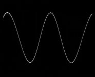
Image 4: 1KHz sine-wave and 30Vpp amplitude.
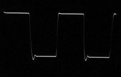
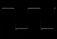
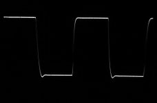
Image 5: 1KHz square-wave and 20Vpp amplitude.
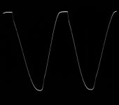
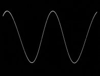
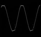
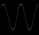
Image 6: 1KHz sine-wave and clipping at 36Vpp.
Image 7: 20KHz square-wave and 20Vpp amplitude.
Image 8: 20KHz sine-wave and clipping at 36Vpp, before amplitude clipping reduction.
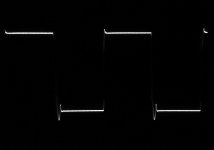
Image 9: 1KHz square-wave, 20Vpp and 68nF directly at the output.
As it is seen from Image 10 with 68nF directly at the output, the TDA2050 still remained stable. 100nF was the limit where permanent oscillation started. The sensitivity to capacitive loading of the TDA2050 is much less than for TDA7293 and LM3886 as examples. For general use, a small Thiele compensation network may still be employed.
A following posting will deal with reduction of the gain to -5 times and -3 times (below the recommended minimum gain). It will also attempt to improve the step response and stability at a gain of -10.
The tests started with a loud “PAAFF”. A 4700uF/35V decoupling capacitor cap left its interior because the grooved top did not open. With only 18V. Such happens when you buy your capacitors too cheap.
Test of the TDA2050 was first done with a gain of -10 (inverting), within the recommended gain range. The results will describe performance for normal use. Further, the current limitation could be investigated.
Image 1: Main components of the amplifier for the first tests.
To start with the current limiter, the TDA2050 is designed such that within the supply voltage range and with a 4 Ohm load, the current limit is only reached near voltage clipping of the sine-wave peaks. The load impedance had to be reduced to 3.2 Ohm and 2.7 Ohm in order to be sure it was current limitation I observed.
The limitation is, as Fred described it in posting #347, a combination of current level clamping and amplitude clipping reduction, probably controlled by the chip temperature. It actually functions quite well in combination but the two effects can be difficult to separate.
It is to be emphasized that the output signal is undisturbed until a bit beyond the peak current level of 5A, unless a high signal level is kept for long such that the chip temperature short after reduces the amplitude clipping level.
The current clamping level was reached some 7% above the 5A limit. With +/-23.5V supply voltage, current clamping was somewhat less controlled and with more instability than when the supply voltage was reduced a bit to +/-22V. +/-22V is a good supply voltage for the TDA2050.
Current clamping of the positive half-waves was almost perfect while clamping of the negative half-waves included a bit of instability, which is less important above the current limit. Soon reduction of the amplitude clipping level would follow. For real music, the current limit of 5A can be relied upon. For a constant sine-wave signal, a level of 4-4.5A should be assumed.
Image 2 shows how an undistorted sine-wave can be started with peak-levels above the 5A limit but just below the current clamping level.
Image 3 shows how the amplitude clipping kicks in some 2-3 seconds later and reduces the power to a sustainable level.
The UTC-TDA2050 can in real use deliver 25W in 8 Ohm and 40W in 4 Ohm, semi-continuously. That is better than the LM1875 and due to better handling of high currents by the TDA2050. An 8 Ohm load was trivial to handle so my results concentrated on 4 Ohm loading.
Results with a regulated +/-22V supply voltage, gain of -22 and a 4 Ohm load.
Image 4: 1KHz sine-wave and 30Vpp amplitude.
Image 5: 1KHz square-wave and 20Vpp amplitude.
Image 6: 1KHz sine-wave and clipping at 36Vpp.
Image 7: 20KHz square-wave and 20Vpp amplitude.
Image 8: 20KHz sine-wave and clipping at 36Vpp, before amplitude clipping reduction.
Image 9: 1KHz square-wave, 20Vpp and 68nF directly at the output.
As it is seen from Image 10 with 68nF directly at the output, the TDA2050 still remained stable. 100nF was the limit where permanent oscillation started. The sensitivity to capacitive loading of the TDA2050 is much less than for TDA7293 and LM3886 as examples. For general use, a small Thiele compensation network may still be employed.
A following posting will deal with reduction of the gain to -5 times and -3 times (below the recommended minimum gain). It will also attempt to improve the step response and stability at a gain of -10.
Attachments
-
 TDA2050_start.jpg17.9 KB · Views: 354
 -
 TDA2050_1KHz_20Vpp_4Ohm_Cap68nFOut.jpg154 KB · Views: 104
 -
 TDA2050_20KHz_Clip36Vpp_4Ohm.jpg210.2 KB · Views: 86
 -
 TDA2050_20KHz_20Vpp_4OhmSQ.jpg125.1 KB · Views: 90
 -
 TDA2050_1KHz_Clip36Vpp_4Ohm.jpg214.1 KB · Views: 83
 -
 TDA2050_1KHz_20Vpp_4OhmSQ.jpg137.2 KB · Views: 330
 -
 TDA2050_1KHz_30Vpp_4Ohm.jpg272 KB · Views: 323
 -
 TDA2050_1KHz_34Vpp_3.2Ohm_3sec.jpg184.2 KB · Views: 331
 -
 TDA2050_1KHz_34Vpp_3.2Ohm_start.jpg298.7 KB · Views: 342
Last edited:
Hi FF
image 10 is missing 😉
Image 10 is actually Image 9. I removed one image at the end and renumbered the image references. I overlooked the mentioning of an Image 10 in the text.
Tomorrow, more images (I hope).
Thanks FauxFrench for the UTC-TDA2050V "exploration" report!
Very informative and interesting documentation.
Looking forward to your upcoming further findings.
Fred
Very informative and interesting documentation.
Looking forward to your upcoming further findings.
Fred
UTC-TDA2050V
Also the TDA2050 starts showing instability (oscillation) on the regular output signal when the gain is reduced below the minimum being recommended (10 times). Oscillation appears less fast than for the TDA7293 which specifies a minimum gain of 20.
The same CR-string as the one used for the TDA7293 was inserted for the TDA2050 and the oscillation stopped. Looking at the square-wave response at 20KHz and varying the values of the string capacitor and the string resistor finally concluded that use of only the resistor without a capacitor gave the best square-wave response.
A resistor between the input pins of 390 Ohm suits a gain of -3 times (2K2/6K5).
A resistor between the input pins of 510 Ohm suits a gain of -5 times (2K2/11K).
A resistor between the input pins of 820 Ohm suits a gain of -10 times (2K2/22K).
With these resistor values, the TDA2050 chip would remain stable down to a gain below -3 and further, the sensitivity to capacitance at the output was importantly improved.
Tests with -3 times gain, +/-22V supply voltage and 4 Ohm load.
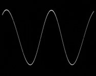
Image 1: 1KHz sine-wave, 30Vpp, 390 Ohm resistor.
Image 2: 1KHz square-wave, 20Vpp, 390 Ohm resistor.
Image 3: 1KHz sine-wave-wave, clipping at 37Vpp, 390 Ohm resistor.
Image 4: 20KHz square-wave, 20Vpp, 390 Ohm resistor.
Image 5: 20KHz square-wave, clipping at 36Vpp, 390 Ohm resistor.
-3dB bandwidth with 4Vpp sine-wave: 400KHz
Output offset voltage: 25mV
Tests with -5 times gain, +/-22V supply voltage and 4 Ohm load.
Image 6: 1KHz sine-wave, 30Vpp, 510 Ohm resistor.
Image 7: 1KHz square-wave, 20Vpp, 510 Ohm resistor.
Image 8: 1KHz sine-wave-wave, clipping at 37Vpp, 510 Ohm resistor.
Image 9: 20KHz square-wave, 20Vpp, 510 Ohm resistor.
Image 10: 20KHz square-wave, clipping at 36Vpp, 510 Ohm resistor.
-3dB bandwidth with 4Vpp sine-wave: 340KHz
Output offset voltage: 35mV
To be continued………………
Also the TDA2050 starts showing instability (oscillation) on the regular output signal when the gain is reduced below the minimum being recommended (10 times). Oscillation appears less fast than for the TDA7293 which specifies a minimum gain of 20.
The same CR-string as the one used for the TDA7293 was inserted for the TDA2050 and the oscillation stopped. Looking at the square-wave response at 20KHz and varying the values of the string capacitor and the string resistor finally concluded that use of only the resistor without a capacitor gave the best square-wave response.
A resistor between the input pins of 390 Ohm suits a gain of -3 times (2K2/6K5).
A resistor between the input pins of 510 Ohm suits a gain of -5 times (2K2/11K).
A resistor between the input pins of 820 Ohm suits a gain of -10 times (2K2/22K).
With these resistor values, the TDA2050 chip would remain stable down to a gain below -3 and further, the sensitivity to capacitance at the output was importantly improved.
Tests with -3 times gain, +/-22V supply voltage and 4 Ohm load.
Image 1: 1KHz sine-wave, 30Vpp, 390 Ohm resistor.
Image 2: 1KHz square-wave, 20Vpp, 390 Ohm resistor.
Image 3: 1KHz sine-wave-wave, clipping at 37Vpp, 390 Ohm resistor.
Image 4: 20KHz square-wave, 20Vpp, 390 Ohm resistor.
Image 5: 20KHz square-wave, clipping at 36Vpp, 390 Ohm resistor.
-3dB bandwidth with 4Vpp sine-wave: 400KHz
Output offset voltage: 25mV
Tests with -5 times gain, +/-22V supply voltage and 4 Ohm load.
Image 6: 1KHz sine-wave, 30Vpp, 510 Ohm resistor.
Image 7: 1KHz square-wave, 20Vpp, 510 Ohm resistor.
Image 8: 1KHz sine-wave-wave, clipping at 37Vpp, 510 Ohm resistor.
Image 9: 20KHz square-wave, 20Vpp, 510 Ohm resistor.
Image 10: 20KHz square-wave, clipping at 36Vpp, 510 Ohm resistor.
-3dB bandwidth with 4Vpp sine-wave: 340KHz
Output offset voltage: 35mV
To be continued………………
Attachments
-
 TDA2050_5x_510R_20KHz_Clip36Vpp_4Ohm.jpg429.9 KB · Views: 71
 -
 TDA2050_5x_510R_20KHz_20Vpp_4OhmSQ.jpg170.8 KB · Views: 71
 -
 TDA2050_5x_510R_1KHz_Clip37Vpp_4Ohm.jpg247.4 KB · Views: 67
 -
 TDA2050_5x_510R_1KHz_20Vpp_4OhmSQ.jpg257.8 KB · Views: 69
 -
 TDA2050_5x_510R_1KHz_30Vpp_4Ohm.jpg322.8 KB · Views: 75
 -
 TDA2050_3x_390R_20KHz_Clip36Vpp_4Ohm.jpg643.1 KB · Views: 76
 -
 TDA2050_3x_390R_20KHz_20Vpp_4OhmSQ.jpg334.3 KB · Views: 70
 -
 TDA2050_3x_390R_1KHz_Clip37Vpp_4Ohm.jpg617.1 KB · Views: 79
 -
 TDA2050_3x_390R_1KHz_20Vpp_4OhmSQ.jpg286.5 KB · Views: 74
 -
 TDA2050_3x_390R_1KHz_30Vpp_4Ohm.jpg309.8 KB · Views: 78
UTC-TDA2050V
Continued from posting #547
Tests with -10 times gain, +/-22V supply voltage and 4 Ohm load.
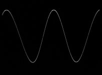
Image 1: 1KHz sine-wave, 30Vpp, 820 Ohm resistor.
Image 2: 1KHz square-wave, 20Vpp, 820 Ohm resistor.
Image 3: 1KHz sine-wave, clipping at 37Vpp, 820 Ohm resistor.
Image 4: 20KHz square-wave, 20Vpp, 820 Ohm resistor.
Image 5: 20KHz square-wave, clipping at 36Vpp, 820 Ohm resistor.
-3dB bandwidth with 4Vpp sine-wave: 260KHz
Output offset voltage: 40mV
When compared with the results in posting #543, also showing results of the TDA2050 with a gain of -10, it is seen that the resistor of 820 Ohm between the two input pins provides increased stability such that the square-wave reproduction at 20KHz is improved with less overshoot. Further and perhaps more importantly, the sensitivity to capacitance at the output is reduced due to the better stability margin.
Gain -3
Image 6: 10KHz square-wave, 20Vpp, 390 Ohm resistor, 100nF capacitor at output.
Image 7: 1KHz, current clamping at 35Vpp in 3.2 Ohm.
The TDA2050 remained stable even with 1uF directly at the output though ringing was very heavy with a square-wave signal.
Gain -5
Image 8: 10KHz square-wave, 20Vpp, 510 Ohm resistor, 100nF capacitor at output.
Image 9: 1KHz, current clamping at 35Vpp in 3.2 Ohm.
The TDA2050 remained stable even with 1uF directly at the output though ringing was very heavy with a square-wave signal.
Gain -10
Image 10: 10KHz square-wave, 20Vpp, 820 Ohm resistor, 100nF capacitor at output.
The TDA2050 remained stable even with 1uF directly at the output though ringing was very heavy with a square-wave signal.
Just using the TDA2050 alone with a gain of -10, I would prefer to add the 820 Ohm resistor, improve stability but perhaps loose a bit of bandwidth.
Continued from posting #547
Tests with -10 times gain, +/-22V supply voltage and 4 Ohm load.
Image 1: 1KHz sine-wave, 30Vpp, 820 Ohm resistor.
Image 2: 1KHz square-wave, 20Vpp, 820 Ohm resistor.
Image 3: 1KHz sine-wave, clipping at 37Vpp, 820 Ohm resistor.
Image 4: 20KHz square-wave, 20Vpp, 820 Ohm resistor.
Image 5: 20KHz square-wave, clipping at 36Vpp, 820 Ohm resistor.
-3dB bandwidth with 4Vpp sine-wave: 260KHz
Output offset voltage: 40mV
When compared with the results in posting #543, also showing results of the TDA2050 with a gain of -10, it is seen that the resistor of 820 Ohm between the two input pins provides increased stability such that the square-wave reproduction at 20KHz is improved with less overshoot. Further and perhaps more importantly, the sensitivity to capacitance at the output is reduced due to the better stability margin.
Gain -3
Image 6: 10KHz square-wave, 20Vpp, 390 Ohm resistor, 100nF capacitor at output.
Image 7: 1KHz, current clamping at 35Vpp in 3.2 Ohm.
The TDA2050 remained stable even with 1uF directly at the output though ringing was very heavy with a square-wave signal.
Gain -5
Image 8: 10KHz square-wave, 20Vpp, 510 Ohm resistor, 100nF capacitor at output.
Image 9: 1KHz, current clamping at 35Vpp in 3.2 Ohm.
The TDA2050 remained stable even with 1uF directly at the output though ringing was very heavy with a square-wave signal.
Gain -10
Image 10: 10KHz square-wave, 20Vpp, 820 Ohm resistor, 100nF capacitor at output.
The TDA2050 remained stable even with 1uF directly at the output though ringing was very heavy with a square-wave signal.
Just using the TDA2050 alone with a gain of -10, I would prefer to add the 820 Ohm resistor, improve stability but perhaps loose a bit of bandwidth.
Attachments
-
 TDA2050_3x_390R_1KHz_CurClip35Vpp_3.2Ohm.jpg238.1 KB · Views: 67
 -
 TDA2050_5x_510R_10KHz_20Vpp_4Ohm_100nF.jpg252.3 KB · Views: 68
 -
 TDA2050_5x_510R_1KHz_CurClip35Vpp_3.2Ohm.jpg275.9 KB · Views: 67
 -
 TDA2050_10x_820R_10KHz_20Vpp_4Ohm_100nF.jpg157.9 KB · Views: 75
 -
 TDA2050_3x_390R_10KHz_20Vpp_4Ohm_100nF.jpg203.5 KB · Views: 76
 -
 TDA2050_10x_820R_20KHz_Clip36Vpp_4Ohm.jpg350.9 KB · Views: 75
 -
 TDA2050_10x_820R_20KHz_20Vpp_4OhmSQ.jpg213.9 KB · Views: 74
 -
 TDA2050_10x_820R_1KHz_Clip37Vpp_4Ohm.jpg304.9 KB · Views: 68
 -
 TDA2050_10x_820R_1KHz_20Vpp_4OhmSQ.jpg169.5 KB · Views: 72
 -
 TDA2050_10x_820R_1KHz_30Vpp_4Ohm.jpg229.2 KB · Views: 70
UTC-TDA2050V
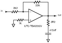
And then, the updated schematic with the main components: Image 1.
The UTC-TDA2050V lived up to my high hopes. The price is very attractive and nevertheless it keeps the promises from the datasheet and can handle importantly more current than the LM1875. With a resistor inserted between the two input pins, the TDA2050 shows convincing stability and impressive tolerance to capacitance at the output. Almost like my “fake” LM1875 but with much higher effective output current and reliable protection features. The protection features are efficient and easy to predict the effect from. The output voltage margins to the supply rails are reasonable.
As I only require little output power (says my wife), the UTC-TDA2050 is a favorite for my next composite amplifier.
I will terminate my assessment of the TDA2050 for now.
Attachments
Yesterday I had my triple LM1875 amplifier in BTL version more-or-less ready and could do a few initial tests. The amplifier uses “fake” LM1875 that in many ways perform quite well, except for the over-current protection feature that cannot be relied upon at all. The amplifier is only implemented as a mono version with six LM1875 ICs (3 in parallel and times 2 for BTL) and using an LM4562 OP-AMP for control.
The amplifier is pretty closely implemented such as described in previous postings and showed no problems except for a very simple soft-clipping circuit (two back-to-back zener diodes) that worked well for the first string but differently for the second string. Finally, I removed this soft-clipping circuit.
The second string was build as a copy of the first string except for the LM4562 coupling that had to be phase-turned 180 degrees compared to the first string. Gains in the three LM1875 were matched and the step-response compared between the first and second strings to be alike.
As written above, over-current protection of fake LM1875 cannot be relied upon. For that reason, I will not test the power capability limit of the amplifier. I fear that if I reach the limit of one (fake) LM1875, that IC will give in and increase the loading on the two other that then will fail as well.
I have tested the amplifier at 1KHz,with +/-24V regulated supply, to 40Vpp in an 8 Ohm load (BTL). That corresponds to 100W at the clipping level. I will try with reduced supply voltage and a 4 Ohm load.
Image 1: BTL-coupling, 1KHz, clipping limit at 40Vpp in 8 Ohm corresponding to 100W.
Image 2: BTL-coupling, 1KHz, 10Vpp in 8 Ohm.
A few more test-results to come.
Attachments


With an 8 Ohm load and 4Vpp amplitude, I measured the bandwidth to 110KHz. The gain was 20dB for each channel, thus 26dB in total.
100nF or even 1uF across the output could hardly be seen on a square-wave. No Thiele compensation network was used.
I checked the triple-BTL 1875 amp with a 4 Ohm load. I did not force it to deliver very high current. The image below shows the output at the level of clipping. 30Vpp in 4 Ohm equivalent to 112W.
Image 1: 30Vpp in 4 Ohm at 1KHz. At the limit of clipping.
Attachments

Last edited:
Hi FF
112Watt into 4R is impressive!
Did you mount all 6 chip to 1 heat sink? did you stack that?
112Watt into 4R is impressive!
Did you mount all 6 chip to 1 heat sink? did you stack that?
Hi FF
112Watt into 4R is impressive!
Did you mount all 6 chip to 1 heat sink? did you stack that?
Hi Chris,
I will post photos of the amplifier tomorrow. It is not really a compact layout due to the many components.
I also implemented an amplitude clamp that worked better.
I have learned a lot from making this 3x2 fake LM1875 amplifier and that was my main goal. I would not do it exactly the same way again. Working with chip-amps that cannot stand over-current is tedious when alternatives with functional protection are available at a fair price. Today, I would use UTC-TDA2050 (2x2) that would do better than fake LM1875 (3x2), or LM3886 (1x2).
If I wouldn't be afraid of blowing the amplifier, I guess it can do more output power than 112W. But, I have another problem - my transformer for the regulated power supply is around 150VA. The supply uses linear regulation.
A class AB amplifier delivering 112W requires some 160W from the power supply. With linear voltage regulation, the transformer needs to supply more than 200W. I simply lack supply power for testing. A future project.
I am about to end this construction and will try my skills in a listening test. I will keep you informed.
After that, I have testing of the genuine LM1875, the TDA7265B, the TDA7292, the OPA549, the LM1876 and the LM4766.
I should then give an improved amplitude clamp some attention.
What are your plans for a composite amplifier?
Hi FF
yes i see your to do list in the other thread...
psu ? i remember your strong regulated psu?..actually distrelec has some transformers at a good price. my brother build his pass F5 with the new bigger PSU boards and a 400VA 18-0-18 transformer - costs about 68euros
300VA 18-0-18VAC 57 euro
%product-title% kaufen
the composite amp is not forgotten by me. i want to go through that because i want to learn how to build this composite e.g. 2x2 1875 or utc
chris
Last edited:
Can you post the final schematic for your 6 chips amp?
Thanks
I will. Most is already posted but I will update the schematics with the few changes and post them again.
They may serve as inspiration to others who also want to try making their own composite amplifier design. It will hardly perform to Neurochrome perfection but well enough to beat most of what you can buy commercially. And, it is not that complicated and suited for medium DIY skills.
- Home
- Amplifiers
- Chip Amps
- LM1875 in parallel configuration and used in a composite amplifier.