H
HAYK
I was new user of Tina when I imported the spice file of 2n7000 and didn't knew how to select the symbol, it remained wrong. The designation of BC327,337 are not aligned.
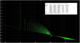
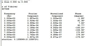
I created the simulation in LTspice XVII, and get 0.001% (10ppm) for 1W at 1kHz into 8R. I had to tweak the current source down from 6.2mA to 4mA to get these results. This is for 46mA of bias on the output devices. If I remove the current source and reset the bias to the same 46 mA, distortion doubles to 0.002%. There is a lot of higher order harmonics though.
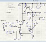
I've attached the asc file. The input network has been simplified and positive rail cap multiplier has been removed, as it shouldn't matter much for a simulation.
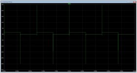
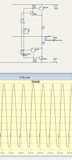
Distortion looks good, but square wave response has significant ringing. Even with a mild 1K signal. Not sure how to address this.
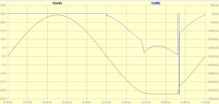
Loop gain looks good with plenty of gain and phase margin (18dB and 75 degrees).
Id did a little bit of testing to see if the optimal current value is dependent on frequency or amplitude. Optimal values did seem to change with amplitude. It might also change with frequency and load. Likely actual device variations as well. This could make it difficult to implement in real life.
I've attached the asc file. The input network has been simplified and positive rail cap multiplier has been removed, as it shouldn't matter much for a simulation.
Distortion looks good, but square wave response has significant ringing. Even with a mild 1K signal. Not sure how to address this.
Loop gain looks good with plenty of gain and phase margin (18dB and 75 degrees).
Id did a little bit of testing to see if the optimal current value is dependent on frequency or amplitude. Optimal values did seem to change with amplitude. It might also change with frequency and load. Likely actual device variations as well. This could make it difficult to implement in real life.
Attachments
H
HAYK
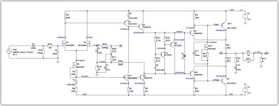
This thread is about the CFP output stage. The P3a that I was using as platform, could not drive with low impedance, so changed the circuit.
As I see you liked so much the amp itself, just as parenthesis from the thread, let me guide you about it.
As you noticed there is no compensation in the amplifying circuit, the dominant pole is in the feedback network made by R20 910ohm and C7 8.2nF places the pole at 20khz. The input must have the same pole to balance, was the 47k and 150pf that you kicked them off. This why you get wrong square waves and if you do AC analysis, you will get flat to 20khz then 6db/octave hike up to maximum open loop gain. The result of this type of feedback, the uncompensated amplifier follows the error signal as its shadow with less than 1us to reproduce extreme high resolution.
Q8 needs high current low saturation transistor, if you don't like my choice a better one is 2n3906 or 2n4402.
In matter of distortion numbers, I showed it is possible with P3a to go down to 0.0005%. The purpose of this amp is not to be instrumentation amplifier but to be sounding beautiful this why distortion numbers up to 0.05% as advertised by Rode Elliot is acceptable. Aska's class A Nirvana has 0.02% and everybody is happy with it. The spectrum of the distortion is more important in this case than the THD number.
Last edited by a moderator:
H
HAYK
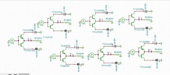
To compare the early Character of power transistors, I made a bench of EF of each pair supplied by triangular current of 1Hz to get about 30v pk on 8 ohms.
Bellow are MJ21193-4, njw0281+0308, njw1302+3281, C5200+a1943, mjl4302+4281 and my actual mismatched njw0281+1302. Finally the c5200+a1943 superposed 5200+njw0302 (shorter).

The old 21193-4 is still a good one for lowest distortion.
The DS of 0281-0302 says they are low power version of 1302+3281 but more linear. Here you can see linear means there early is identical.
Bellow are MJ21193-4, njw0281+0308, njw1302+3281, C5200+a1943, mjl4302+4281 and my actual mismatched njw0281+1302. Finally the c5200+a1943 superposed 5200+njw0302 (shorter).
The old 21193-4 is still a good one for lowest distortion.
The DS of 0281-0302 says they are low power version of 1302+3281 but more linear. Here you can see linear means there early is identical.
Attachments

Last edited by a moderator:

H
HAYK
I tried on Tina the 21193-4 and c5200+0302. Indeed with Onsemi mjl model I got the 0.029% and C5200+0302 ,0.05% more second harmonic on open loop 20Vpk 24 ohm source.
I will continue with the 21193-4. It has sufficient harmonics and requires 24 ohms, nested feedback with 2Mohm.
I will continue with the 21193-4. It has sufficient harmonics and requires 24 ohms, nested feedback with 2Mohm.
H
HAYK
I have noticed the Cordell models for the MJL1302C, MJL3281C and MJL4281C, MJL4302C have RE=0.0 and this does not give the same Gm plot as the datasheet. Someone else has also mentioned this independently to my finding. The MJL21193C has RE=0.001 and MJL21194C has RE=0.01 and these look too low, but I haven't checked them against their datasheet.
To get more a realistic model for Gm I use RE=0.03 for the MJL1302C, MJL3281C and MJL4281C, MJL4302C. Possibly RE=0.03 for the MJL21193C, MJL21194C as well until confirmed.
Normally with large value emitter resistors in typical amplifiers this RE=0.0 discrepancy is insignificant for THD etc. But when you test the transistors without any emitter resistance, like your jig above, it gives significant differences compared to datasheets and a real transistor.
H
HAYK
Good morning Ian.
I noticed great difference between the LT and Tina behavior. First, the 2SD669 CCS measures 44ma on LT but 30ma on Tina!!.
I brought my MJ21193-4 Pspice files from Tina to LT and compared to what Minek had, much different whereas the MJL version which should be identical has double Hfe that should. Bellow is comparison of mine upper and Minek which has unbelievable PNP.

I added bellow mines.
I restarted back on LT with these files, immediately it showed difference in Vbe that I had to increase the base resistor of NPN to 160 ohm. Normally it is less than 5%.
The model started behaving as one expect from a push pull to have low 2nd harmonic. The crossover is near perfection.

I ordered from Ali 2 pairs genuine for $15 and another pair for $1.6 original but defective. Sometimes the defect is plastic issue.
I noticed great difference between the LT and Tina behavior. First, the 2SD669 CCS measures 44ma on LT but 30ma on Tina!!.
I brought my MJ21193-4 Pspice files from Tina to LT and compared to what Minek had, much different whereas the MJL version which should be identical has double Hfe that should. Bellow is comparison of mine upper and Minek which has unbelievable PNP.
I added bellow mines.
I restarted back on LT with these files, immediately it showed difference in Vbe that I had to increase the base resistor of NPN to 160 ohm. Normally it is less than 5%.
The model started behaving as one expect from a push pull to have low 2nd harmonic. The crossover is near perfection.
I ordered from Ali 2 pairs genuine for $15 and another pair for $1.6 original but defective. Sometimes the defect is plastic issue.
Attachments
H
HAYK
I was wondering why Rode Elliot changed from NPN to PNP VAS to call the P3, P3a.
As I deduced, the CFP has more gain negatively, if that is the goodness, then, NPN vas would be better. Transistors pull more than release. By inverting he reduces, even over turns the gain ratio. In the last version with EF add, my distortion for 20Vpk 24 ohm Impedance is 0.05% but nearly equal 2nd and 3rd harmonics. This is not what should be.
I took back the Darlington VAS, replaced it with BD140 and pulled 40ma to get 20 ohm Impedance and 0.13% distortion. I repost bellow the CFP distortion of MJ21193-4 to add with that of the driver. Add? I must say subtract because the phases of the 2nd and the 3rd are opposite. The balance 2nd -3rd can be adjusted by the CCS of the VAS.
Attachments

Oops, Re: my comment in Post 87 on your jig in Post 86.
I just noticed you are current driving the transistors with no bias voltage. This means you are using current drive and therefore the dominant gain parameter is Beta (HFE) and not their Gm. So whether the models emitter resistances are RE=0.0 or RE=0.03 it won't affect your jig plots.
Sorry I didn't notice that at first.
H
HAYK
I have a problem with the OPS. It doesn't want to saturate on negative rail. To be sure it is not the driver I replaced it with A1220 and paralleled a pair with 3 ohm emitter resistors. In vain, I replaced the PNP output with njl better but not as good as the positive side. Can it be the spice model not to the spec which shows less than 1V sat. for 15A?
I found a Japanese website full of transistor spice models, you name it, there it is.
http://www.cyada.org/oto/audio/spice/bjt.html
Edit. I add with 4 ohms load, the blueish the driver collector current.
I found a Japanese website full of transistor spice models, you name it, there it is.
http://www.cyada.org/oto/audio/spice/bjt.html
Edit. I add with 4 ohms load, the blueish the driver collector current.
Attachments
Last edited by a moderator:
H
HAYK
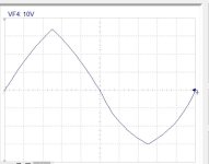
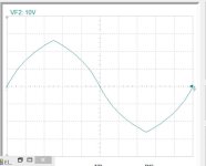
Second harmonic phase effect in time domain.
I added to a sine wave its second harmonic of 10% with relative phase shift of 0°,90°,180°,-90°and-180° shown bellow from top to bottom.
Remark that -180°and 180° are the same.
Each shift alters the sound presence, staging.

I added to a sine wave its second harmonic of 10% with relative phase shift of 0°,90°,180°,-90°and-180° shown bellow from top to bottom.
Remark that -180°and 180° are the same.
Each shift alters the sound presence, staging.
H
HAYK
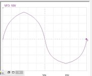
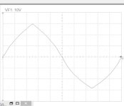
This is the 3rd harmonics added the same sequence as for 2nd order. Now it is clear that the 3rd becomes dirty sounding when it is other than in phase (1) or opposite (3&5).

That Japanese web site has several model libraries which are quick to download from here:
https://www.cyada.org/oto/audio/08spice.html
I was playing with CFP circuits with gain and noticed that the PNP 2955 caused clipping for lack of gain and limited driver current. Of course, that depends on the load impedance etc. One of the chip amps uses CFP to get the most out of 12VDC and the limited gain as a current limit protection.
The CFP is interesting because you can use it to get rail-rail output from an op-amp IPS, otherwise, I would stick with EF2,3 . My circuit uses current mirrors instead of base resistors and gets close to 0.001%THD in ~class-B, and clips very close to the rails, but it uses 8 driver transistors so I dunno if it's such a great idea.
Attachments
H
HAYK
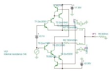
Hayk,
Interesting idea above. But adding T2 and T6 Darlington makes the CFP oscillate. Reducing the Beta of T2 and T6 is stable but pullout transistors T7,T8 also need lowered Beta's.

This cross-coupling links the two halves together so the current source cannot keep one side slightly on anymore. The current source is not needed and can be removed.
Also this cross coupling forms a translinear loop down to DC that biases the output transistors without the need for the emitter resistors R14, R16 (I have reduced them to be a short). By stepping the temperature of power transistors Q7, Q9 you can see the crossover current is unaffected by their temperature 😉 . Stepping of the CFP driver transistors Q6, Q5 is temperature sensitive which is surprisingly stable with no emitter resistors (and they are compensated with the bias spreader Q5).
Q16,Q19 and Q17,Q20 pairs are cascoded by Q12, Q13 so they operate at low Vce and low dissipation. These pairs provide a doubling of current to drive the power transistors so the CFP driver transistors Q6, Q5 run slightly cooler than the previous basic CFP drivers. Likewise Q10,Q14 and Q11,Q15 run cool).
As for high frequency charge pull-out it is quite effective without needing to carefully choose capacitors (or inductors) as in my previous methods.
It also seems to be an improvement on the Wim de Jagger bias loop (eg here) at high frequencies since the above method allows slower power transistors to be stable over temperature with no emitter resistors or thermal feedback of the main heatsink (as mentioned only the drivers Q6,Q8 need compensation). The problem with the the Wim de Jagger bias loop is no charge pull-out for the power transistors so very fast power transistors are needed (80MHz). BTW Q10 is paralleled with Q18 for double charge pull-out for the PNP power transistor compared to the NPN. Also these mirror transistors need emitter ballasts (10 ohms?) since discrete's are never 100% matched. Likewise Q16,Q19 and Q17,Q20 pairs need ballasting and mirror pairs like the BCV61/62 might help.
A nice idea. It may be a winner? What do you want to call it?
Cheers, IanH
Interesting idea above. But adding T2 and T6 Darlington makes the CFP oscillate. Reducing the Beta of T2 and T6 is stable but pullout transistors T7,T8 also need lowered Beta's.
This cross-coupling links the two halves together so the current source cannot keep one side slightly on anymore. The current source is not needed and can be removed.
Also this cross coupling forms a translinear loop down to DC that biases the output transistors without the need for the emitter resistors R14, R16 (I have reduced them to be a short). By stepping the temperature of power transistors Q7, Q9 you can see the crossover current is unaffected by their temperature 😉 . Stepping of the CFP driver transistors Q6, Q5 is temperature sensitive which is surprisingly stable with no emitter resistors (and they are compensated with the bias spreader Q5).
Q16,Q19 and Q17,Q20 pairs are cascoded by Q12, Q13 so they operate at low Vce and low dissipation. These pairs provide a doubling of current to drive the power transistors so the CFP driver transistors Q6, Q5 run slightly cooler than the previous basic CFP drivers. Likewise Q10,Q14 and Q11,Q15 run cool).
As for high frequency charge pull-out it is quite effective without needing to carefully choose capacitors (or inductors) as in my previous methods.
It also seems to be an improvement on the Wim de Jagger bias loop (eg here) at high frequencies since the above method allows slower power transistors to be stable over temperature with no emitter resistors or thermal feedback of the main heatsink (as mentioned only the drivers Q6,Q8 need compensation). The problem with the the Wim de Jagger bias loop is no charge pull-out for the power transistors so very fast power transistors are needed (80MHz). BTW Q10 is paralleled with Q18 for double charge pull-out for the PNP power transistor compared to the NPN. Also these mirror transistors need emitter ballasts (10 ohms?) since discrete's are never 100% matched. Likewise Q16,Q19 and Q17,Q20 pairs need ballasting and mirror pairs like the BCV61/62 might help.
A nice idea. It may be a winner? What do you want to call it?
Cheers, IanH
Attachments
Last edited:
H
HAYK
Since I discovered the class D in ABD modulation with its extreme resolution, I am interested in analog ones only in those that the class D cannot achieve (without DSP).
If you want this one, you can have it and deposit a copyright.
I am working since one year, probably my last analog amp, an equivalent in solid state of Luxman MQ68C. This tube amp lunched in 1979 was the last model using 50C10, a triode based on an old US one but much more non linear, designed and manufactured only for Luxman. The amp generates 0.3% THD mainly 3rd harmonic of opposite phase and this from 0.1W to 25W in open loop, 0.05% with 16db NFB in closed loop. Luxman replaced it recently by MQ86 using KT88 in triode, without much success.
At this stage, the circuit is autobiased and non switching but consumes 35W at quiescent as four MOSFETs needs to be biased 250ma each to get 0.3% +/-0.03. Normally such distorting amp is of no any interest on this website but using a derived driver from Chatharsis, it can work in open loop, 16NFB and very high NFB to bring the THD very low level.
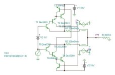
Hayk,
You wrote in the above post : "If you want this one, you can have it and deposit a copyright."
Are you referring to my circuit in Post 96? The circuit based on your circuit in Post 95.
I'd be interested in further developments of it, maybe I can start a new thread for it? If you are not interested in more in this thread that is.
Cheers, IanH
H
HAYK

H
HAYK
I received $1.60 pair of MJL21193_4,
https://www.aliexpress.com/item/1005004394552144.html
The are not polished inscription, just mat. They measure B_E 0.521V and 0.531V. They look genuine but the back plates aren't flat, mater of scrubbing on sand paper.
https://www.aliexpress.com/item/1005004394552144.html
The are not polished inscription, just mat. They measure B_E 0.521V and 0.531V. They look genuine but the back plates aren't flat, mater of scrubbing on sand paper.
- Home
- Amplifiers
- Solid State
- Linearizing the CFP crossover - P3a of Rod Elliot as example