H
HAYK
The temperature model of BD139 is probably modeled after Siemans DS which shows a drift of less than 100mv from 25 to100°C instead of 150mv. I tried the low impedance circuit with BD139 ST and BC557B, it did follow perfectly 2mv/°C. Assuming that both drivers are dissipating the same power and cooled identically, then the Vbe transistor can be mounted on one of the drivers without NTC on the other. The temperatur variations of the assisting transistor has no effect.
Attachments
Agreed, from memory decreasing the emitter R below the stated value, may not be a brilliant idea.Interesting, having built a P3A i feel the urge to experiment, I also notice you reduced the emitter resistors to 0,05ohm from the original 0,33ohm is there a specific reason for that?
When looking at it I also wonder how necessary it is to use a constant current generator, the VBE variations of the output transistors would be very small compared to the total 70V supply voltage, could you just use a 12K resistor instead?
I was certainly not able to do it with my P3A using paralleled output stage without problems - it was back in 2008, so I can't recall what issue it caused.
H
HAYK
The P3a doesn't have the drivers temperature compensation even not hearsinks I suppose. The Vbe multiplier is separate alone. Only the emitter resistors limit the bias hike but it surely increases. In my case the Vbe multiplier reads the junction temperature and compensates. I have a good knowhow in this subject.
Does it not?
The temp co. is compensated (in part) by the mounting of the driver transistors.
Edit:
Actually let me correct myself, the driver transistors are mounted on their own heatsinks (in my case) the diode multiplier transistor is glued to the output heat sink.
I think this is the temp co. Compensation suggested by Rod Elliot (I repeat that it has been some 15 years since I looked at the design in any depth so my familiarity with the design is relying on memory)
i used both BD139/140 and the suggested MJE340/350 altwenatives. I stuck with the MJE, because i could heat sink those easily.
Output devices were Bourns TIP2955/3055, with the best Ft available for those parts (again, if i recall, 2.5MHz).
I never used big Toshiba BJTs, because, well that wouldnt be a P3a amplifier any longer, and it was my feeling that the big Toshibas would need a stronger driver transistor.
Rod suggests BC547/557C (I forget which) and not BC 550C which is not quite the same beast, lower noise, and gain (IIRC)
No it is not perfectly compensated, but it isn't terrible, and there isn't a huge problem with temp co.
I don't feel that simulation is going to live up to reality, which is usually the case.
Last edited:
H
HAYK
It is a mistake to compensate the main heatsink. The Vbe multiplier should be glued upon one of the drivers directly upon the transistor. In fact, R.Elliot didn't design the output stage, he copied it, I suppose, from D. Self's book as it uses 0.33 ohms.
http://www.douglas-self.com/ampins/dipa/dipa.htm
http://www.douglas-self.com/ampins/dipa/dipa.htm
The big Toshiba outputs don’t require a stronger driver. If anything they let you get away with one that is more delicate. All the Toshiba types have far higher gain above 2 amps than anyone’s version of a 2955/3055. Less driver current is required, not more.i used both BD139/140 and the suggested MJE340/350 altwenatives. I stuck with the MJE, because i could heat sink those easily.
Output devices were Bourns TIP2955/3055, with the best Ft available for those parts (again, if i recall, 2.5MHz).
I never used big Toshiba BJTs, because, well that wouldnt be a P3a amplifier any longer, and it was my feeling that the big Toshibas would need a stronger driver transistor.
But it wouldn’t really be a P3A anymore. It may needs some compensation changes. With EFs you can always substitute a bigger faster output with no problems or changes required, at least as far as stability is concerned. Not necessarily so with CFPs. You take those on a case by case basis.

H
HAYK
I am looking for better driver transistor. I saw LJM using D699 B649 pair. Hitachi has stopped once upon a time these but numerous other sources are available. This pair is enhanced BD139,140 with higher voltage but most important, the Ic/Vbe is perfect square law up to 100ma where I need in worst case 50ma. A better version of this pair is NEC's C2690/A1220 and the Fairchild version with higher early, now available from Onsemi as KSC/KSA.
I was lucky today to find from a nearby vendor original Hitachi ones, NEC 2sa1220 and Fairchild C2690 with equal Hfe to NEC of 208. Measuring the B+C-E both pairs have exactly the same diode voltages.
I downloaded the spice models from Onsemi, unfortunately it doesn't work well, for D699/B649, I couldn't find any.
*The Fairchild is isolated.
Attachments
H
HAYK
I found model for 2sc2690 posted by@kct.
Post in thread 'Spice models for 2SC2690' https://www.diyaudio.com/community/threads/spice-models-for-2sc2690.334682/post-5715725
Any idea where look for 2sa1220?
Post in thread 'Spice models for 2SC2690' https://www.diyaudio.com/community/threads/spice-models-for-2sc2690.334682/post-5715725
Any idea where look for 2sa1220?
I have these:
.MODEL KSA1220 PNP IS=4.7863E-13 BF=289.3 BR=9.76 NR=1.006 ISE=5.2481p NE=2 ISC=2.4909E-11 NC=1.5 VAF=98.5 VAR=6.7 IKF=2.7061 IKR=0.0759 RB=2.26 RBM=0.2308 IRB=0.001 RE=0.1908 RC=1.1748 QCO=0.02 RCO=3.9811 VO=11.078 GAMMA=5.01187E-8 CJE=3.4786E-10 VJE=0.9575 MJE=0.4694 FC=0.5 CJC=1.1224E-10 VJC=0.5761 MJC=0.4365 XCJC=0.4955 XTB=1.7978 EG=1.2255 XTI=3
.MODEL KSC2690 NPN IS=1.7783E-13 BF=132.5 BR=8.495 NR=1.005 ISE=1.9953E-13 NE=1.5 ISC=1.5849n NC=1.98 VAF=580.75 VAR=18.15 IKF=4.0271 IKR=0.012 RB=2.98 RBM=0.001 IRB=0.6396 RE=0.0909 RC=1.4705 QCO=0.68 RCO=3.6239 VO=6.587 GAMMA=2.8216E-7 CJE=4.0082E-10 VJE=0.6696 MJE=0.3296 FC=0.5 CJC=6.0404E-11 VJC=0.5 MJC=0.4266 XCJC=0.4955 XTB=1.2590 EG=1.2277 XTI=3
.MODEL 2SD669A NPN ( BR=0.0116 CJE=1.5E-10 CJS=0 EG=1.11 FC=0.5 IKF=0.403 IKR=1 IRB=1E-06 IS=6.73f ISC=1E-13 ISE=1.14E-14 ITF=9.99 MJC=0.407 MJE=0.33 NC=2 NE=1.04 NF=0.8 NR=1.03 RB=4 RBM=0.761 RE=0.00255 TR=0 VAF=25.1 VAR=50 VJC=0.3 VJE=0.75 VTF=1E +06 XTB=3.82 XTI=2.5 BF=3.350000E+02 CJC=6.110000E-11 RC=5.550000E-01 TF=9.010000E-10 XTF=4.450000E+01)
.model 2SB649A pnp ( IS=293.5f BF=216 NF=1.0 VAF=40 IKF=1.5 ISE=101.1p NE=2.6797 BR=7 NR=1.0 VAR=20 IKR=0.05 ISC=1.345p NC=1.5558 RB=0.46 RBM=0.46 RE=5m RC=1.07 CJE=295.4p VJE=0.6977 MJE=0.5197 TF=0.8569n XTF=53.4 VTF=2.83 ITF=1.22 CJC=113.1p VJC=0.5466 MJC=0.5742 XCJC=0.5 TR=14.65n XTB=1.87 EG=1.11 XTI=3.0 FC=0.5)
.model NTE373 ako:2SD669A
.model NTE374 ako:2SB649A
Modern NTE373/4 are probably re-badged UTC versions of D669/B649. They have to get them from somewhere since they don’t actually MAKE anything. They will not be the original Hitachi or anything NEC, since those OEMs don’t make them anymore. Unless they were sitting on a distributor’s shelf since 1985 (not likely but possible).
How about Toshibas current offering TTA004B and TTC004B? They are avalible from the big distributors in large numbers.
TTA004B Mouser
TTC004B Mouser
Edit: Toshiba have spice models on their home page:
https://toshiba.semicon-storage.com...oduct/bipolar-transistors/detail.TTA004B.html
https://toshiba.semicon-storage.com...oduct/bipolar-transistors/detail.TTC004B.html
I am not the master simulator driver but I will ty to import them to LTspice.
Last edited:
Nothing wrong with them at all. They are one of their old NLA 2SA/2SC TO-220 pairs stuck in a TO-126 case.
H
HAYK
Thank you Minek, thank you very much for the 2SB,2SD models. The KS ones are the same from Onsemi, not good. I will modify the working 2690 version into PNP and adjust the parameters, maybe it work.
The TTA/TTC 004b have strange Ic/Vbe curve that doesn't resemble to square law. In linear scale an exemplary square law curve is that on the DS of C5200, whereas with Ic logarithmic scale, power becomes slope and on 2SB/2SD DS, it is perfect straight line from 1ma to 100ma. It is not the case in BD139/140 DS, figure3 Vbe(on) in pdf bellow.
Attachments
The linearity of an output transistor in application depends on the linearity of the load which it presents to preceding stages. In your case your outputs are on the line between voltage and current driven by the CFP drivers. If they were only collector driven it would be pure current drive but adding the B-E resistor shifts it toward voltage drive.
Ic/Ib (beta) is a linear relationship and is much more linear than Ic/Vbe in the transistor's optimal range. Therefore driving a base with a collector is usually the most linear arrangement. However when you add a B-E resistor, the the current drawn through this resistor by Vbe becomes a nonlinear load on the driver transistor.
The extent of this nonlinearity depends on where the output transistor is in it's dynamic emitter resistance curve. If the dynamic emitter resistance is very low as in high collector current, then there will be little Vbe swing and so the current swing through the B-E resistor will be small compared to the swing of Ib. In this case we are still effectively in current drive because the B-E resistor contributes minimally to the load current swing of the driver transistor, and so it's harmonic contribution is minimal.
If the dynamic emitter resistance is very high as in low collector current, then the Vbe voltage swing will be high and the resulting current swing through the B-E resistor will be the majority of load current swing on the driver transistor collector. Because Vbe is very nonlinear, the load current will be nonlinear and this nonlinearity will be propagated backwards through the feedback mechanism and appear in the LTP differential voltage as it must drive all the proceeding stages which may be nonlinear.
The Ic point where the output transistor + B-E resistor transitions from exponential to linear sensitivity depends on Beta, and the B-E resistor value. When the dynamic emitter resistance is equal to the B-E resistor divided by Beta, the current swing of Ib and the B-E resistor will be equal (for small stimulus). Therefore:
Ic(transition) = 27mV/(Rbe/Beta)
So if your output transistor has a Beta of 100 and Rbe is 100, then the transition from exponential to linear sensitivity will occur at Rm=1ohm or 27mA.
This will also be the Ic where sensitivy drops to half. Therefore if we want our sensitivity to be the same at crossover as it is at excursions, this is our optimal bias current, because when both NPN and PNP outputs are operating at the same time our sensitivity will both added together. So at the crossover point both will be at half sensitivity, but since they are in parallel their sensitivities will add. And then at excursions when one output turns off, the other one is at full sensitivity. This mirrors the Oliver criteria for EF output stages where optimal crossover behavior occurs when the emitter resistors have 27mV bias. And unfortunately, this output scheme will have the same wiggle in it's transfer curve because it's the same mathematical function.
Earlier you noticed the NJW1302 showed more linear behavior in simulation. I don't fully trust manufacturer SPICE models, but the effect you noticed could have been because the model has very low Hfe, shifting the transition to nonlinear behavior to a lower Ic. You could replicate this effect with other transistors by increasing Rbe.
The linearity of this way of driving a BJT is very dependent on Hfe, so you can expect your results to vary as much as Hfe does from part to part. Furthermore, the tempco above the transition point depends on Hfe whereas the tempco below the transition point depends on Vbe, so now you have the wonderful complexity of having to ensure nothing bad happens in either condition. At bias your tempco will be some highly variable combination of Beta and Vbe tempco which may require individual adjustment for each build. Imagine bouncing back and forth between a tempco trimmer and a bias trimmer to get everything to line up, waiting a few minutes between each adjustment to see if the tempco compensation is good.
One huge advantage of the EF output stage is consistency and not being dependent on something as variable as Hfe.
H
HAYK
Waow, what a literature for such a simple thing.
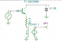
To see simple, it is just a common collector circuit which will generate a current from a voltage source. The asymptotic gm of the circuit is defined by the emitter resistance. As my collector current is amplified by the output 100 times, the driver sees the resistance 100 times higher, 0.05 ohms as 5 ohms. To make a perfect crossover joint the bias should have a slope, that is gm half the asymptot which is 0.2S. The driver then itself will be 0.2S too to result 0.1S. Bellow is the simulation of this circuit driven by a triangular wave 50 Hz 0.5v offset. The scope shows the half slope occurs with 2sc2690 at 12ma. So simple.


To see simple, it is just a common collector circuit which will generate a current from a voltage source. The asymptotic gm of the circuit is defined by the emitter resistance. As my collector current is amplified by the output 100 times, the driver sees the resistance 100 times higher, 0.05 ohms as 5 ohms. To make a perfect crossover joint the bias should have a slope, that is gm half the asymptot which is 0.2S. The driver then itself will be 0.2S too to result 0.1S. Bellow is the simulation of this circuit driven by a triangular wave 50 Hz 0.5v offset. The scope shows the half slope occurs with 2sc2690 at 12ma. So simple.
Attachments
Last edited by a moderator:
I do not understand what is strange in the TTC004 looks to be as good as 2SD699 to me, here is the Ic/Vbe curve cut out from datasheets of TTC004, 2SD699 and BD139, BD139 looks worst to me.


H
HAYK
The TTA curve is saturation curve, the figure 7.6 Ic Ib is to look at. Same for D669, it is also sat curve.
I find the concept very interesting: it is extremely simple and highly effective, unlike many similar "keep-alive" schemes.
Those schemes are either purely decorative, or worse, they add nasty artifacts of their own.
Two remarks:
I don't see why the CFP allows smaller emitter resistors: 1mV mismatch between the base-spreader and the junctions to compensate will result in the same current; OK, the number of junctions is different etc., but it doesn't seem to justify the 100 factor.
It would be nice to have the complement: this fix addresses the conduction issues, but the turnoff can also be problematic especially with BJT's. With a darlington output, a coupling of the bases with a 1µF heelps the turnoff, but in a CFP it is more complicated.
I have even tried small transformers to cross-couple the bases, but it didn't work satisfactorily.
Anyway, your scheme is a worthwhile innovation, bravo for that!
- Home
- Amplifiers
- Solid State
- Linearizing the CFP crossover - P3a of Rod Elliot as example