Most manufacturers tell us to NEVER use the opamp offset nulling pins to null out an input offset error coming from the Source................Pity it doesn't have dc offset nulling pins to null out any dc coming into it from the source, as it gives vey low dc offset itself.
Cheers George
You either DC block that Source and go to the Source and correct the offset error there.
And what should normally be done to the unused offset nulling pins? Should they just be left open or connected to gnd/supply?
Thanks,
Oleg
Thanks,
Oleg
Thanks Chris!
I just got curious because many op-amps have no nulling pins and because in this case they are NC (Not connected) I connected them to gnd on my PCB... So I'll have to disconnect them just in case if I encounter an op-amp with nulling pins...
I just got curious because many op-amps have no nulling pins and because in this case they are NC (Not connected) I connected them to gnd on my PCB... So I'll have to disconnect them just in case if I encounter an op-amp with nulling pins...
Hi Oleg,
You may be fine, but I have a healthy distrust that a datasheet might hold for all sources. Besides, if you later want to change that IC to something else, it would be nice if you didn't have to do surgery on your PCB.
That was a very good question, I'm glad you asked it.
-Chris
You may be fine, but I have a healthy distrust that a datasheet might hold for all sources. Besides, if you later want to change that IC to something else, it would be nice if you didn't have to do surgery on your PCB.
That was a very good question, I'm glad you asked it.
-Chris
Yeah, cutting traces on a PCB is not nice... I just left floating pin 1 and pin 5 of a single op-amp (8 pin SOIC) package. Pin 8 is still connected to positive supply for shorter pass from the supply decoupling cap to pin 7. I guess I'll have to keep it this way and just remember to cut off pin 8 from an op-amp before soldering.
Thanks for your help!
Oleg
Thanks for your help!
Oleg
Almost there, again...
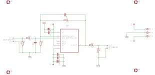
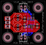
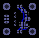
Some time ago I've been almost ready to submit my buffer PCB for manufacturing but then I started tweaking it again and here is what it is now (see attached). I have separated the PSU from the buffer/preamp. And now I have even more questions.
1. Is it OK to overlay the power traces (top side: red) over the signal path (bottom side: blue) as I did it?
2. I also see that sometimes the ground plane has an opening just below the op-amp on some of the PCBs. Should I be concerned about it? And what would be the reason for such an opening in the ground plane?
3. On my board the signal ground is connected to the power ground using a single via between pins 1 and 8 under the op-amp. Is it sufficient connection between the power and signal ground?
Thanks,
Oleg
Attachments
Hi Oleg,
1. They would be capacitively coupled, so you wouldn't want to do that. Run the common return under a power trace and the signal return under a signal trace. Or just use one side as a ground on the signal side. Keep the power return common separated from the ground plane.
2. The opening is to minimize high frequency loss. A ground plane can cause instability near the input side of the op amp circuit.
3. Depends an awful lot on the circuit or the entire system. To create a low impedance connection for grounds (or supplies or anything else) use multiple vias - many. A single via can be inductive as its a cylinder the length of the board's thickness. This may or may not present a problem for you.
I guess there are a lot of "it depends" in circuit design. But no one section can be designed without regard to how the entire system will be connected. That's where standard ways of hooking your stuff up can come in really handy. You don't design something different every time, you just follow the plan.
-Chris
Thanks a lot Chris!
Now it seem like an impossible to do from geometrical point of view🙂 I guess it would be way easier to implement on a 4 layer PCB: top - power, then power return plane, next signal ground plane and finally signal on the bottom. And then connect the two inner ground planes together where appropriate. But unfortunately I'm limited to a two layer PCB.
I have to think now how to reroute the signal and the power with its return. If I put power return under the power traces I'll have to lift the signal to the top layer and make a lo-o-o-ong loop around the IC for the feedback connection on top of the PCB.
By the way is it a problem to route the feedback all the way around the IC or it is better to use a dual op-amp and use only single channel of it (e.g. replace the LME49990 - my initial idea - by the LME49720)? This way all ins and out are on the same side of the IC.
Also power pins are more conveniently located.
Actually how much is too long for the feedback connection path? I know people are using DIP package ICs with through-hole resistors where distances are much larger than it would be around the SOIC package. Should I really be concern about it in my case?
Thanks,
Oleg
I'll have to think... may be I'll manage to solve this puzzle...
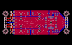
While playing with the PSU design I've got a question if it is really necessary to have CRC filter before the regulators? I understand that in high current PSU with lots of capacitance it is a good thing (CLC being even better) but what about PSU delivering ~50mA / 12VDC for most of its life?
Thanks,
Oleg
Yeah leave it in. CLC is nicer and you'l be sure that no garbage can creep in. I would add the rectifier diodes to the PSU to make life simpler when installing the boards. The reasons to use coils in high current PSUs are very different than in a low current preamp design.
BTW I think I spot a classic design mistake... I see an RC filter direct in front of the opamp. With a volume control before that RC filter you'll have a filter with varying -3dB point. The RC filter should be before the volume control.
I see you trust on your chain to be DC offset free. I think you might regret that. At the output it won't be a problem with LME49990 (the power amp has input caps ?) but I would include input caps just in case. You can short them in case your sources are DC free but in real life chances are that at least one of your sources carries more DC offset than you would like.
Last edited:
Most manufacturers tell us to NEVER use the opamp offset nulling pins to null out an input offset error coming from the Source..
You either DC block that Source and go to the Source and correct the offset error there.
Barrie Gilbert told me no problem on his AD844, so long as it's not excessive.
Cheers George
AndrewT is right, you don't correct a problem of a preceding stage by introducing a technical non optional solution in the next stage. Always solve it at the source of the problem/challenge certainly with different sources that might carry different offset voltages. You'll be having various DC offset voltages introduced by yourself otherwise 🙂
And where is the limit of "excessive" ? 100 mV ? 1 V ?
And where is the limit of "excessive" ? 100 mV ? 1 V ?
Last edited:
Hi Jean-Paul,
The design has "slightly" changed now. I have separated a PSU (attached) from the buffer. Because I have a relay based R-2R attenuator DC is not a problem as long as it is blocked at the entry to the amp and there I have a DC blocking cap.
Regards,
Oleg
The design has "slightly" changed now. I have separated a PSU (attached) from the buffer. Because I have a relay based R-2R attenuator DC is not a problem as long as it is blocked at the entry to the amp and there I have a DC blocking cap.
Regards,
Oleg
Attachments
It still is good design practice to filter out DC before the opamp....just like the RC filter should be before the volume control. Filtering DC is a good idea to avoid plops when switching sources. Please think about that. You don't want the "moving woofer syndrome" do you ? 😉
BTW you will have problems soldering in connectors in the PSU board as the screws will likely touch the plastic part of the connectors. The board looks nice but why no coils ? You could use them at the bottom of the board to gain space (this also count for resistors). Heat won't be a problem in this application. With more board space the LME49990 can be on this very board saving some tedious wiring and possible future bad connections (wenn's nicht falsch gehen kann geht's nicht falsch 🙂)... You can skip one pair of decoupling caps and the PSU output connector when the opamps are very close to the regs with their output caps.
And please add a 0.1 µF cap directly at the pins of the opamps from their + to their - power supply pins. You will like the result.
Last edited:
Hi Oleg,
It's all a puzzle, designing PCBs. The art of compromise where you don't get to have anything the perfect way. 🙂
I see we have a couple other smart guys helping you now. Their information is very good too.
-Chris
It's all a puzzle, designing PCBs. The art of compromise where you don't get to have anything the perfect way. 🙂
I see we have a couple other smart guys helping you now. Their information is very good too.
-Chris
Yeah...! I noticed the attention. Although desired it also makes me feel like a young student... again🙂
Jean-Paul,
The head of the screws that I use does not touch the white circle surrounding the mount pad. So there should not be a problem mounting the boards without touching the connectors. I also tried fitting there a 2.54mm pitch molex connector and it seems to have enough clearance too. Buy the way what type of coils would you recommend for max 200 mAmps current? I am not so familiar with parts.
Regarding the buffer on the same board (initial idea) - if I figure out how to do the buffer routing right I'll probably revisit this possibility. So far it seems to be easier to make a PSU right as a stand alone board.
Regards,
Oleg
OK, no problems with the screws. Seemed a little tight to me.
I use ELJ-FB101JF from Panasonic a lot but they're out of production now (still available though) and they are only 105 mA. Are you sure your preamp needs so much current ? 200 mA seems a lot to me.
Regarding the routing, I have to read all info but I guess you could use the connector you now use for the output voltages for the in- and outputs. As a member of the non-modular PCB design committee I can only tell that wiring is not my hobby (to put it mildly). Better design that single non-compromise board you'll be proud of. You'll be invited to be a gold member of the committee too then !
Last edited:
If I move the RC filter before the volume control. Do I still need a small series resistance before the op-amp input in this case?
Thanks,
Oleg
Thanks,
Oleg
- Status
- Not open for further replies.
- Home
- Source & Line
- Analog Line Level
- Line level buffer: discrete or ICs based?