Hi John,
Can you explain Fig. 8 in the datasheet of OPA1642? It shows a sharp rise of distortion if a source resistance is added above 1kHz.
Have you measured something other? Maybe the AD797 from analog , which is one of the rare opamps free from common mode distortion?
Best,
Udo
Can you explain Fig. 8 in the datasheet of OPA1642? It shows a sharp rise of distortion if a source resistance is added above 1kHz.
Have you measured something other? Maybe the AD797 from analog , which is one of the rare opamps free from common mode distortion?
Best,
Udo
This is actually not a 100% correct statement. All op amps will produce some amount of distortion in the non-inverting configuration with a source impedance mismatch at the two inputs. For bipolar and dielectrically isolated JFET-input amplifiers it requires a "worse" circuit for the effects to show up.
These effects come from non-linear input impedance and pretty much all op amps have a source of non-linear input impedance, here are some of the offenders:
Bipolar op amps:
- ESD Diode junction capacitance
- Mismatch in ESD diode leakages
- Collector-Base Capacitance (can be mitigated with input stage cascode)
- Beta of input devices varies with VCE (can be mitigated with input stage cascode)
JFET-Input Op Amps:
- ESD Diode junction capacitance
- Mismatch in ESD diode leakages
- Bottom gate to substrate variable capacitance (mitigated in DI processes)
- Gate to source and gate to drain capacitance(can be mitigated with input stage cascode)
CMOS Op Amps:
- ESD Diode junction capacitance
- Mismatch in ESD diode leakages
I've taken A LOT of measurements on this, and come to the conclusion that in the voltage follower configuration, a source impedance mismatch will always degrade performance slightly. The best parts that I've measured so far are our modern JFET input parts (OPA140/141/1641 and OPA827) followed by the older DiFET parts (OPA627, 2107, etc.) followed by bipolar amplifiers with modern CMOS amps close to bipolars (OPA1652, OPAx172).
Some of these measurements (for JFET-input parts) are shown in this article: http://www.ti.com/lit/an/slyt595/slyt595.pdf
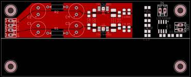
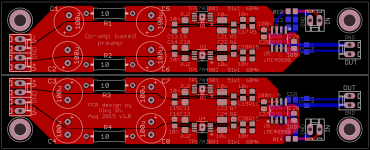
First PCB draft
I have played with the schematic and the PCB layout. So far only the PSU section is routed (see attached). I have followed the evaluation board layout for the TPS regulators. The resistors R1 and R2 are just placeholders. Most probably I'll place there the common mode filters or the ordinary inductors.
The pre-regulators will be off board.
The entire PCB is 10x4 cm and has the footprint of my R-2R attenuator PCB (mount holes, IN and OUT location). The plan is to make it dual mono. So far only one channel is in progress. The other will follow. Don't be confused by the amount of resistors around the op-amp in the schematic. Not all will be used at once.
If someone sees an obvious or not so obvious problem with the regulators layout please let me know.
Regards,
Oleg
Attachments
Hi Keruskerfuerst,
Most probably the layout that you see made you think I need an education in the PCB design... which is 100% true. But could you please be more specific? So far I did not do anything fancy, just more or less copied the layout from the TPS7A49/30 evaluation board from TI. I followed their suggestion not to use vias and place components on one side of the PCB. The op-amp is not even routed yet. So the local decoupling etc is not there. May be in the schematic I should have placed C13/14 next to the op-amp supply pins but I will just do it on the PCB... Anyways, I am learning by doing and I do read about the subject... but may be not enough. I do not try to pretend to know the thing... and I am trying to follow advice as good as I can.
Any suggestion which helps to improve the design?
Thanks,
Oleg
Hi John,
Can you explain Fig. 8 in the datasheet of OPA1642? It shows a sharp rise of distortion if a source resistance is added above 1kHz.
Have you measured something other? Maybe the AD797 from analog , which is one of the rare opamps free from common mode distortion?
Best,
Udo
Fig 8 in the datasheet of the OPA1642 was taken before a process improvement was made and the datasheet has not been corrected. The measurements on the OPA1642 that I gave in my article are on the current version of the product. The entire OPA1642 datasheet is slated to be updated soon, so stay tuned 🙂
John,
While we have you here, a question about the OPA1612, which has great specs and a price to match. I found on Aliexpress a lot for 2.15 USD/piece, and I bought some. Is there an acid test to determine they are real or fake? Can look to around -110 dB distortion with my present setup, but would rather have something easier than increasing noise gain.
While we have you here, a question about the OPA1612, which has great specs and a price to match. I found on Aliexpress a lot for 2.15 USD/piece, and I bought some. Is there an acid test to determine they are real or fake? Can look to around -110 dB distortion with my present setup, but would rather have something easier than increasing noise gain.
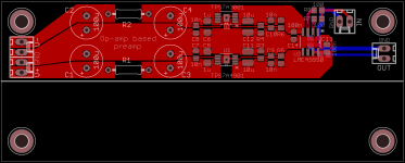
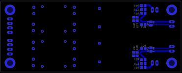
PCB design progress
Half of the PCB is done (see attached). Slightly updated the schematic with some components values. The other half of the PCB (second channel) will be symmetric.
Just to remind you, the intention is to allow using the board in the inverting or non-inverting configuration with or without the gain. So not all resistors around the op-amp will be populated. Some will be jumpers or empty depending on the situation.
Please let me know if I missed something or may be if something is totally wrong. May be there are missing important components... or other problems. I'm still learning. So please comment!
Regards,
Oleg
Attachments

Just a thought
Would be nice to incorporate for 8 pin dual in line dip socket as well to experiment with different plug in opamps.
Cheers George
Would be nice to incorporate for 8 pin dual in line dip socket as well to experiment with different plug in opamps.
Cheers George
Hi George,
I agree that it would make the PCB even more versatile but it would require a lot of extra traces length because dip sockets do not aligne with the smd pads and need to be rotated by 90 degrees to fit without overlap. This would "disturb" the layout a lot.
I agree that it would make the PCB even more versatile but it would require a lot of extra traces length because dip sockets do not aligne with the smd pads and need to be rotated by 90 degrees to fit without overlap. This would "disturb" the layout a lot.
OlegSh,
To pick it up where Kuersterfuerst left it.
Some things would make it better:
* Why did you include R7? This is highly unconventional and this kind of connection between the two inputs of an op amp is normally only made to increase noise gain in order to get measure distortion that would normaly be below the measuring instruments limit. Better drop it.
* It is good custom to put a small capacitor over the feedback resistor to limit gain at high frequencies. This increases stability.
* On the input side, you want to put a small cap after the 100Ohm input resistor to filter out radio frequencies.
Your regulator side looks good to me, and the RC filter at the input is a nice feature.
Hi vacuphile!
Thanks a lot for the hints! This is really helpful!
I'll add a capacitor after R8 to ground for RF attenuation. Also will add a capacitor across the feedback resistor. Should these capacitors be in the range of tens of pF? I guess the RC value combinations should give me some hundreds of kHz limit or what value should I design for?
The R7 is there for the inverting configuration (the value indicated on the schematic is the result of copy/paste, please ignore). I may as well drop the entire inverting configuration part. Haven't decided yet. It is always easy to leave the pads not populated. It makes no harm and takes little space.
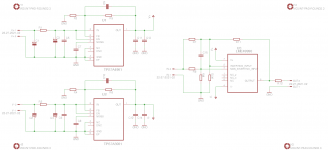
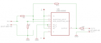
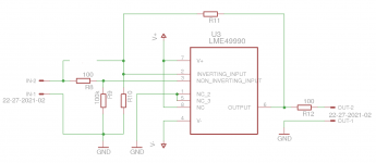
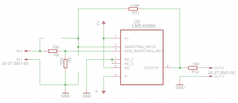
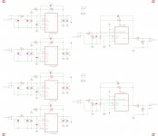
Please see below the reduced schematics showing only necessary parts for each configuration.
From left to right: non-inverting unity gain; non-inverting with gain set by 1+R11/R10; inverting with gain set by -R11/R7, and if I understood it right R9 should be equal to R7//R11 for minimum output offset but everywhere I see it, it is just a 0 Ohm link. I will have to read more to understand what to do with it. Suggested capacitors are still missing, but I'll add them ...
Please let me know if missed something.
Regards,
Oleg
Thanks a lot for the hints! This is really helpful!
I'll add a capacitor after R8 to ground for RF attenuation. Also will add a capacitor across the feedback resistor. Should these capacitors be in the range of tens of pF? I guess the RC value combinations should give me some hundreds of kHz limit or what value should I design for?
The R7 is there for the inverting configuration (the value indicated on the schematic is the result of copy/paste, please ignore). I may as well drop the entire inverting configuration part. Haven't decided yet. It is always easy to leave the pads not populated. It makes no harm and takes little space.
Please see below the reduced schematics showing only necessary parts for each configuration.
From left to right: non-inverting unity gain; non-inverting with gain set by 1+R11/R10; inverting with gain set by -R11/R7, and if I understood it right R9 should be equal to R7//R11 for minimum output offset but everywhere I see it, it is just a 0 Ohm link. I will have to read more to understand what to do with it. Suggested capacitors are still missing, but I'll add them ...
Please let me know if missed something.
Regards,
Oleg
Attachments
Last edited:
OlegSh,
Opinions differ, but if you calculate a - 3dB point @ 100 KHz for the feedback cap, I think you can't go wrong. In case of unity configeration with Rf=0 Ohm, a cap would make no sense as you rightly suppose.
About R7, now I understand you did this to keep flexibility to use it in an inverting setup, that makes sense. Op amp distortion in the non-inverting setup gets higher with unmatched source impedances, so inverting is technically better. However, since in the inverting setup the source resistance of the gear you connect to the preamp will influence the gain, it is not very practical. But to have the option won't hurt.
Thanks vacuphile!
So in the end my ideas were not too bad. I just had a moment of frustration before your previous post... thanks for giving me confidence. It is my first op-amp based circuit so I wasn't sure if I got it right. Also I apologize for removing the stupid question from my previous post about the capacitor parallel to the wire (R11=0) which you answered. Should have thought of it before doubting🙂
Thanks again for your help!
Regards,
Oleg
I've finally finished the PCB layout. I dropped the idea of inverting/non-inverting possibility and went with non-inverting only. The updated schematic and the PCB layout are attached below. I'll wait a bit just in case any kind of optimization will come to mind and then order the PCBs.
Thanks everyone who contributed!
Oleg
Thanks everyone who contributed!
Oleg
Attachments
While playing with the PSU design I've got a question if it is really necessary to have CRC filter before the regulators? I understand that in high current PSU with lots of capacitance it is a good thing (CLC being even better) but what about PSU delivering ~50mA / 12VDC for most of its life?
Thanks,
Oleg
Thanks,
Oleg
- Status
- Not open for further replies.
- Home
- Source & Line
- Analog Line Level
- Line level buffer: discrete or ICs based?