kartino said:Hi sawreyrw,
Even it built from junk part. UcD is the only for 'poor' DIYer.
Best Regards,
kartino
LOL
😀 😀 😀 😀 😀 😀 😀 😀 😀 😀
poor eh 😀 😀 😀
just dont have the patience ordering those parts overseas.. might take a month of waiting....

 😀
😀 might as well use parts locally available....
I guess your right, UCD is the only choice for me.... 🙂
I was planning to make the "thunderball" scheme BUT would like to change the IR chip(lever shifter) into dicscrete parts (transistors/common ICs).. if only i knew HOW.... 😉 😀
Hello,
RX5, yes UCD is a discrete circuit, no IC, I agree with Kartino of course, it is the perfect poor man's DIY project, and as I said before, the end results are highly worth it. Other benefits are it really could not be much simpler, so you dont' even need to scavenge that many parts. It also simulates rather well.
Several have had good results building their own already. Some put more effort into it than others and consequently leart more... it's really up to you.
A good thread to start with is diy reference design.
A number of application notes describe the high side mosfet issue. Search google for discrete gate drivers and mosfet basics/power switching. It's alot to take in, there's alot to learn, dont' expect to get there overnight.
The problem is that the mosfet responds to signals from the gate with reference to the source, and with a high side N channel the source is floating on the output, therefore, so must your high side gate driver .
There's a surprising number of ways in which to achieve this, many having been covered in the forum, many more on google.
The simplest is a type of charge pump known as a bootstrap. Then there's the matter of level shifting, also a number of ways of going about that... some are even a 2 birds with one stone solution. Best of way of finding them all is some hard research.
Regards
Chris
PS: Thanks to those who have been encouraging to learn lately, I think it will make all the difference.
Hi RX5,
Hom big your amp output? 100-200W the best choice is UcD concept. 500W use IR reference, over 1kW ask Fredos, 😎 enter to pro audio.
Hom big your amp output? 100-200W the best choice is UcD concept. 500W use IR reference, over 1kW ask Fredos, 😎 enter to pro audio.
RX5, keep that power level as an end goal.... but start out with something like 35 to 50W first. One little step at a time.

Yes.
Where'd you find that? Should really post a reference instead of just lifting the picture and asking us what we think... this is not research! Do you have any specific questions in relation to it?
I'm not too fond of it myself.
Where'd you find that? Should really post a reference instead of just lifting the picture and asking us what we think... this is not research! Do you have any specific questions in relation to it?
I'm not too fond of it myself.
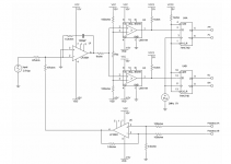
I found it when i was searching google for broken car class d amps, more specificly here: http://ece.wpi.edu/analog/mqps/
the circuit in post #191 will work, if R2 resistor is between Q1's emitter, and Q1's collector. Then, that resistor will pull up Q1, so Q1 can charge the upper mosfet's gate. When Q4 is ON, then Q4 will pull down Q1-Q5, and the upper mosfet's gate will be discharged by Q5. I have made a similar "discrete high-side driver", and it works.
I use for this position BCX53/BCX56.
In Q4's position I used to use BSS17, but I will try BSS123. It's a SOT23 packaged FET.
I use for this position BCX53/BCX56.
In Q4's position I used to use BSS17, but I will try BSS123. It's a SOT23 packaged FET.
Tekko,
So you've read this then http://ece.wpi.edu/analog/mqps/ClassD_MQP_Final.pdf
and chose to ask if we've seen "this type of modulation"? Did you read it? There's nearly 200 pages of information for you there... what is the type of modulation?
This is what I'm saying when I said if you research you should at least get to an informed question.
Danko, gold star for you then. Can you imagine why everyone else suggested it be simulated though. You should too, because it's still not going to work.
I spent hours reading the 100 pages worth of info there, finished sometime after midnight.
3-level Sigma Delta modulation, supposed to run cleaner and sound better.
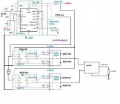
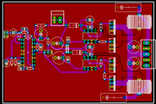
It seems very simple in schematic level but its not, it is very hard and i mean hard to make a board for this. It is impossible not having signals cross each other, which would ruin the amps performance as it is operating @ 2MHz.
I emailed a professof on the website asking if they had any board layouts left but they dident, tho they said that i might had wanned to improve grounding if they would have had layouts still,
so i´m left out by myself.
I would want to make one, but my eagle skills doesent allow me.
3-level Sigma Delta modulation, supposed to run cleaner and sound better.
It seems very simple in schematic level but its not, it is very hard and i mean hard to make a board for this. It is impossible not having signals cross each other, which would ruin the amps performance as it is operating @ 2MHz.
I emailed a professof on the website asking if they had any board layouts left but they dident, tho they said that i might had wanned to improve grounding if they would have had layouts still,
so i´m left out by myself.
I would want to make one, but my eagle skills doesent allow me.
You'd be going down an expensive road leading to a dead end again.
What would you have learnt if he did have a PCB for you, and you had the parts to plug into it? Will there always be a PCB available for download for your circuits?
I have never designed a PCB myself, but if I had a circuit worthy of it, and the financial means to do so, I would sure figure it out pretty fast.
I can get all parts, the most expensive one would be the HIP4081, it costs around €3 which isent mutch, the other components are just cheap everyday food.
If you read the pdf, you see that this circuit is tested and all component values are calculated for optimum performance so even a n00b should be able to put one together with having a readymade pcb made from the schematic, with addition to some 0.1µF bypass caps between the ic Vcc and gnd legs.
The only thing i cannot get is the chosen fets, but IRFZ44 seem to be good enuf.
But this till be a later project when i have learned to use eagle more efficiently. For now i´ll protoboard Worhorse´s schematic with SG2524 and IR2111, he have approved the schemo i wipped together based on his schemo and given me the the goahead to move on to prototyping stage.
Attachments
-Just out of curiosity, how do you intend on prototyping this as the "next stage"?
-What's your budget for this project?
-What's your end goal? Do you expect this design will achieve it.
-At what point will you give up on it (cost overrun, boredom.. ??)
Don't set yourself up to fail.
Oh, and post #213.....
Do you seriously expect that a "fully optimized and tested" with a "should be good enough" pair of mosfets will work swimmingly .. for a "noob"?
What happened to your last circuit again when you tried a "should be good enough pair of mosfets"? It got expensive suddenly.... didn't it. Conclusions?
Look back to the start of this thread and see how many times you were tipped off to read data sheets. Find the app notes you need to find so that you may understand what they mean and what to look for on them..
That's research, not finding another PCB to download.
This time im convinced that it´ll work without a hitch, IR2111 have more deadtime allowing the fets to never cross conduct, actually too mutch deadtime but as it will be a subwoofer amp only, that wont really matter.
I´ll continue as long as i have money. I think i have enuf money to even buy one of fredos´s biggest amps.
I won´t quit.
I´ll continue as long as i have money. I think i have enuf money to even buy one of fredos´s biggest amps.
I won´t quit.
😀 You're dead serious, aren't you?Tekko said:This time im convinced that it´ll work without a hitch
So I guess you're designing a PCB for this now?
I've done all I can do here.
First a protoboard test to see if the schemo have any spririt of life in it.
I wish i could make my own dual layer boards, i have no stuff to do that.🙁
I wish i could make my own dual layer boards, i have no stuff to do that.🙁

Right on!~
You actually can make a dual layer board of sorts... worry about that after you get it going on the board though.
There is a guy here in sweden that makes double sided boards, but he uses these through hole plating repair rivets, how good are these ?
- Status
- Not open for further replies.
- Home
- Amplifiers
- Class D
- level shifters and mosfet drivers