A well used and indispensable tool for the shop is a reliable power supply. Some of the features I would like to incorporate into the design:
- Adjustable voltage. As planned, 0 - 30VDC
- Isolated dual supplies, independently adjustable that can be used on their own or put in series to form either a split 30VDC supply or a single 60VDC. When put in parallel, the 2 supplies can give double the current.
- Adjustable current limit for both supplies.
- Built in analogue voltmeter and ammeter on both supplies.
- Built in current limited receptacle. Current limiter in this case is a regular incandescent light bulb in series with the mans. This is for first powering up external power supplies. The bulb will have a bypass switch.
I may think of more along the way 🙂
I actually started this project a while ago (familiar story...😀) but stalled. I have a supply that I built a couple years ago and have been using that. It has some short comings:

With its lid off. One cheap digital ammeter one one leg of the split supply.
So,
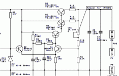
Start with the circuit:

One channel shown, both channels are identical. I didn't know for sure if it with work as planned. It worked well in simulation but that doesn't necessarily mean it will in reality. As I only have a minimum of actual knowledge, it is yet another cobbled together circuit, drawing upon several sources - a "patchwork" power supply I guess.
Today I built a prototype and ran it.
- Adjustable voltage. As planned, 0 - 30VDC
- Isolated dual supplies, independently adjustable that can be used on their own or put in series to form either a split 30VDC supply or a single 60VDC. When put in parallel, the 2 supplies can give double the current.
- Adjustable current limit for both supplies.
- Built in analogue voltmeter and ammeter on both supplies.
- Built in current limited receptacle. Current limiter in this case is a regular incandescent light bulb in series with the mans. This is for first powering up external power supplies. The bulb will have a bypass switch.
I may think of more along the way 🙂
I actually started this project a while ago (familiar story...😀) but stalled. I have a supply that I built a couple years ago and have been using that. It has some short comings:
With its lid off. One cheap digital ammeter one one leg of the split supply.
So,
Start with the circuit:
One channel shown, both channels are identical. I didn't know for sure if it with work as planned. It worked well in simulation but that doesn't necessarily mean it will in reality. As I only have a minimum of actual knowledge, it is yet another cobbled together circuit, drawing upon several sources - a "patchwork" power supply I guess.
Today I built a prototype and ran it.
It looks a bit complicated and it is but functionality first, simplicity second.
First thing I discovered today after I ran the prototype: I don't have enough current at the base(s) of the pass transistors. Current to the load during testing was maxing out at ~800mA. To increase this I think that R1 and R2 need to be a lower value, to pass more current as needed.
Voltage adjustment is incredibly linear and smooth. For the prototype I'm using a multiturn trimpot and I think I get panel mounted multiturn pots for the final version.

In the background (among the mess) are the meters I'll use.
First thing I discovered today after I ran the prototype: I don't have enough current at the base(s) of the pass transistors. Current to the load during testing was maxing out at ~800mA. To increase this I think that R1 and R2 need to be a lower value, to pass more current as needed.
Voltage adjustment is incredibly linear and smooth. For the prototype I'm using a multiturn trimpot and I think I get panel mounted multiturn pots for the final version.
In the background (among the mess) are the meters I'll use.
On second thought...it's probably best to limit the amount of current that is drawn from the doubler supply. Ripple will undoubtedly go up if I increase the draw.
I feel I may need to either switch the pass transistors to darlington or add a "driver" stage to increase the gain. I think I'll go with a driver, since I don't have any power darlingtons here:

It shouldn't be too difficult to add it to the prototype board for a trial run.
Also, 2 pass transistors is probably overkill here and I may eliminate one and with it, both of the emitter resistors.
I feel I may need to either switch the pass transistors to darlington or add a "driver" stage to increase the gain. I think I'll go with a driver, since I don't have any power darlingtons here:
It shouldn't be too difficult to add it to the prototype board for a trial run.
Also, 2 pass transistors is probably overkill here and I may eliminate one and with it, both of the emitter resistors.
Last edited:
Adding the driver fixed the problem. There is enough gain to easily drive the load. I used MJE15030 for this because I have many of these and no other use for them at the moment.
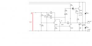
The revised schematic:

I have deleted the second pass transistor. I think one MJL21194 can easily handle any load this supply will see. Heatsinked and current limited to a max 2A, it should be fine.
Voltage regulation is outstanding. Searching for multiturn pots on Digikey had me looking at units from $20 right up to $150! Who would pay this much for a 5 turn pot? NOT me, I'll either use a single turn or create a shaft attachment for a multiturn trimpot.
I haven't really tested out the current limit yet. I know it functions but I need to see if it has the variability I want. One concern is Q6 - it may need to be changed to a larger device. When the supply is in current limit, Q6 sinks the overload current from the base of Q1. Milliamps only but maybe too much dissipation for a TO-92.
The revised schematic:
I have deleted the second pass transistor. I think one MJL21194 can easily handle any load this supply will see. Heatsinked and current limited to a max 2A, it should be fine.
Voltage regulation is outstanding. Searching for multiturn pots on Digikey had me looking at units from $20 right up to $150! Who would pay this much for a 5 turn pot? NOT me, I'll either use a single turn or create a shaft attachment for a multiturn trimpot.
I haven't really tested out the current limit yet. I know it functions but I need to see if it has the variability I want. One concern is Q6 - it may need to be changed to a larger device. When the supply is in current limit, Q6 sinks the overload current from the base of Q1. Milliamps only but maybe too much dissipation for a TO-92.
Some fiddling with the current limit and I've found that R12 needs to be halved, from 6K down to ~3K (I used 2.7K). Some explanation (as best I can):
R12, D5 and R17 provide voltage for the base of Q6, through pot R18. Rotating pot R18 counter clockwise (less current) increases the voltage at the base of Q6. This in conjunction with the voltage drop across current sense resistor R16, turns on Q6 sinking current from the base of Q1, thus reducing the voltage. Current at the output stays constant as the voltage drops.
By reducing R12, I increased the "threshold" voltage (for want of a better term) giving better variability near the end (max current) of the current adjust pots travel. To fine tune this I will put a 500R trimpot in series with R12.
As usual, I was wrong. Reducing R12 was the wrong move and I should have seen it. Sufficient to say that 6K for R12 is still a bit too low. The supply goes into current limit before pot R18 is fully counter clockwise. Ideally, it should hit "0" before that happens, Full scale operation of the pot is what I'm after.
Making R12 8.2K plus a trimpot in series should do the trick. I found that 10K was too high, limiting the low end of the current limit to ~300mA at 30V output.
Making R12 8.2K plus a trimpot in series should do the trick. I found that 10K was too high, limiting the low end of the current limit to ~300mA at 30V output.
Ok, I have it sorted out:

Quite a bit of monkeying around and I have it where it should be. Current limit goes from a low of 150mA @ 30V to 2.1A at maximum setting - excellent!
At lower voltages, it is possible to set the current limit even lower, to 100mA. I am pleased with this result.
I have made a couple other changes: Added a trimpot in series with the adjust resistor for the LM317. It allows the reference voltage to be set to exactly 15VDC. This will in turn limit the output voltage to exactly 30VDC. I also changed the grounding location for the LM317 to the rectifier side of the sense resistor.
Next is to do a new board layout.

Ahh , "men of action" at work... only 30V ?? I need a dual 0-50V setup instead of my crude trafo/bridge/ELcap setup. Your looks similar to the Nico "ELD" ps (below). I am trying an IC-less regulated design with a current sourced Zener (you hate zeners - but 317's have 4 of them).
OS
OS
Attachments
(you hate zeners ...
I got over that 🙂
Hey OS,
30 volts is fine for 99% of the testing and prototyping I'll do. If more voltage is needed (like for a completed amp ready for serious testing), I would build the supply that powers it. I think it is a bit wasteful to construct a supply with high voltage and current capability unless it's getting used constantly.
I'd suggest you move the connection of the anode of D2 to the positive output of D3 to make sure C3 won't be reverse-biased a lot during startup. That C3 is so small looks pretty strange too. Using a C3 much smaller than C1 doesn't make much sense unless you are using its reactance to keep the "doubled" voltage down. But an electrolytic capacitor is not going to like that kind of treatment.
Why did you change the negative sensing of the LM317? The way it is now the reference voltage to the voltage regulator decreases with increased output current, making the output impedance even larger than R17 itself at maximum output voltage.
You may also want to add reverse polarity protection diodes across the pass transistor(s) and the output. A diode in series with the base of Q1 might be useful too so the transistors can't be destroyed during downprogramming by current from capacitors or batteries connected to the output. A diode over R17
A base-"discharge" resistor is then needed for the driver and the compensation should prefereably be connected to the output side of the diode to speed up recovery.
Have you made sure voltage regulation isn't lost during turn-on and turn-off? It looks like the pass transistors will go full-on when the main bus voltage drops to about 3-4V if the doubled supply still has charge left. On the other hand most circuits will survive a 3V output...
The current limiter isn't going to have very good regulation, ripple and temperature stability specs but it's not worse than many other DIY PSU circuits. Do you really want the weak foldback characteristic given by R21 or is it perhaps tuned to counteract the early effect in the current limit transistor?
I'd suggest you move the connection of the anode of D2 to the positive output of D3 to make sure C3 won't be reverse-biased a lot during startup. That C3 is so small looks pretty strange too. Using a C3 much smaller than C1 doesn't make much sense unless you are using its reactance to keep the "doubled" voltage down. But an electrolytic capacitor is not going to like that kind of treatment.
Hi Mega,
The value for C3 was just arbitrary, enough to get the doubler to work, given the low current demand on this part of the supply. I could easily use 100uF there but increasing it (in simulation) didn't have any positive effect so I just went with the 10uF. Although the schematic shows a polarized cap, I'm using a bipolar in the prototype, so not worries of it reverse biasing.
Why did you change the negative sensing of the LM317? The way it is now the reference voltage to the voltage regulator decreases with increased output current, making the output impedance even larger than R17 itself at maximum output voltage
I thought it was the other way round - that it would be better to have the LM referenced to the supply side of the sense resistor. "true" 0 volts exists there, on the load side of the sense resistor the "0" volts fluctuates with current demand. ???
You may also want to add reverse polarity protection diodes across the pass transistor(s) and the output. A diode in series with the base of Q1 might be useful too so the transistors can't be destroyed during downprogramming by current from capacitors or batteries connected to the output. A diode over R17
My original had a diode across the output but it got lost somewhere during revisions. I'll squeeze it in or mount it across the binding posts.
A diode to protect R17 - will do.
The current limiter isn't going to have very good regulation, ripple and temperature stability specs but it's not worse than many other DIY PSU circuits. Do you really want the weak foldback characteristic given by R21 or is it perhaps tuned to counteract the early effect in the current limit transistor?
The current limiter is more of a protection mechanism. I wanted to be able to set the max limit to a reasonable amount for the circuit being tested and I think it does that well enough.
Ripple is very low, even under heavy load. 2 to 3mVpp with a moderate load (400-500mA) is pretty good. Many will look at this and see the doubler and think this is nothing but a 120Hz oscillator - this is not the case.
Temp stability is yet to be determined. A little shift one way or the other is not a big deal for me though.
R21 is supposed to foldback the current output slightly (a bit less than the max current output) during a short circuit on the output. I have not actually tried it out and 3K may not be the most suitable value.
Thank you for the suggestions!
I'll tinker with it a bit more and implement them.
🙂
Looks like one sentence got cut off there... 😛 A diode across the output would protect a turned-off supply if you put it in series with another one or if there is a short rail-to-rail when using two as a split supply.
The diode across output transistors would be for protecting the transistors if you connect a battery to the output or put two supplies in parallell and turn off one. I'd add a diode over R17 too because the peak current (in the reverse direction!) could be pretty high when charging the input capacitor from the output and that could be unhealthy for the resistor itself but also the current limit circuit connected to it. Maybe I worry too much.
If it is not a precision current regulator that you need then your current limiter looks fine to me. The voltage regulator is pretty nice, but I'm pretty sure you want the reference voltage referenced to the negative output. You could just try your prototype with a load at high output voltage and see what happens. If I'm not mistaken the LF output impedance will be about 1 ohm.
If you want to lower the ripple it might help to add an R-C filter to the base drive supply, but your 1 mF capacitor there is pretty big considering the current draw so I guess it may not be needed after all.
I'd still suggest you add something to protect the output transistor, driver and "VAS" transistor if a voltage source is connected to the output because the "VAS" transistor would turn full on if the external voltage is higher than the programmed voltage. You'll get reverse breakdown in the driver and maybe the output transistor too and lots of current through the "VAS". A diode in series with the driver base would mitigate that.
Last edited:
Member
Joined 2009
Paid Member
Mega you are a taskmaster! All good though as I know that you are giving me excellent advice, as you have done many times in the past.
I have implemented the changes:

Hopefully I got everything correct.
In the sim, with the LM317 grounded to the load side of the sense resistor, there is fluctuation in the reference voltage with a load applied. Connection at the supply side and there is no fluctuation. I haven't had a chance to check this out on the prototype yet and I'm not sure which way I grounded it on there.
I have implemented the changes:
Hopefully I got everything correct.
In the sim, with the LM317 grounded to the load side of the sense resistor, there is fluctuation in the reference voltage with a load applied. Connection at the supply side and there is no fluctuation. I haven't had a chance to check this out on the prototype yet and I'm not sure which way I grounded it on there.
John,
Looking good.
I see my heatsink being put to good use again 🙂
Gareth! Howdy 🙂
That was the first and last project I did with your🙂D) heatsink. The majority of the 2 meter length is still untouched. I'm sure I'll find some use(s) for the rest of it.
Board revised to the above scheme:

Not on the board id D8. This will be soldered directly to the legs of Q2.
Last edited:
Have you looked at dissipation requirements when high current is required from one or both supplies at low output voltage?
A multi-tapped transformer will help a lot in reducing the heat dissipation load.
Even a 115:0,10,20,30+0,10,20,30Vac transformer would massively reduce heat load.
A multi-tapped transformer will help a lot in reducing the heat dissipation load.
Even a 115:0,10,20,30+0,10,20,30Vac transformer would massively reduce heat load.
pcb layout
sir MJL21193 im just new to pcb making can i ask what is the software you are using for making the pcb layout...
sir MJL21193 im just new to pcb making can i ask what is the software you are using for making the pcb layout...
😛 Thanks!
I take it you mean the voltage between the output pin of the LM317 and the negative terminal of the bridge changes. That is inconsequential however as what you need constant really is the voltage between the LM317 output pin and the negative output terminal. You want the current sense resistor R17 to be "outside" the voltage regulating circuit.
It may be easier to see if you remove the current limiting circuitry or just define the negative output as ground. The negative terminal of the bridge then has a negative voltage that depends on the current drawn. This unwanted disturbance gets added to your reference voltage if you keep the current connection of the reference voltage regulator negative sensing lead.
Attachments
- Status
- Not open for further replies.
- Home
- Amplifiers
- Power Supplies
- Lab Power Supply Design / Build